
Low power consumption logic cell

Active Publication Date: 2017-06-22
COMMISSARIAT A LENERGIE ATOMIQUE ET AUX ENERGIES ALTERNATIVES
View PDF35 Cites 11 Cited by
  • Summary
  • Abstract
  • Description
  • Claims
  • Application Information

AI Technical Summary

Benefits of technology

The patent describes a logic cell for an integrated circuit that includes a first variable-capacitance capacitor and a third control electrode. The third control electrode can receive a control voltage to change the capacitance between the first and second main electrodes. The cell also includes a second variable-capacitance capacitor and a hold circuit for supplying a logic output signal. The power supply voltage can be a DC voltage or a variable periodic voltage. The first and second capacitors can have a positive or negative capacitance variation, and can be micro- or nanoelectromechanical. The capacitance variation can be achieved by varying the surface area, distance, or dielectric constant of the main electrodes. The cell has leakage currents smaller than 1 nA and preferably smaller than 1 pA. The patent also describes a series association of multiple logic cells.

Problems solved by technology

Logic cells based on transistors assembled as resistive bridges however are limited in terms of electric power consumption.
However, in practice, the decrease of the power supply voltage goes along with an increase of leakage currents in transistors, and thus of the static power consumption of cells.
In practice, adiabatic logic circuits formed in CMOS technology are also limited in terms of power consumption.
In particular, since a MOS transistor always has a non-zero threshold voltage, there inevitably remains a residual non-adiabatic power dissipation for each switching of the cell transistors.
The decrease of the threshold voltage of transistors in advanced CMOS technologies enables to decrease such a non-adiabatic dynamic power dissipation, but generally goes along with an increase of leakage currents, and thus of the static power consumption of the cells.
In practice, the use of microelectromechanical or nanoelectromechanical switches however raises issues.
Indeed, such switches often have relatively high on-state resistances, particularly due to the poor quality of the electric contact between the fixed conducting portion and the mobile conducting portion of the switch.
This causes an additional power dissipation which partly cancels the gain provided by the implementation of an adiabatic logic.

Method used


Image

  • Low power consumption logic cell
  • Low power consumption logic cell
  • Low power consumption logic cell

Examples


first embodiment

[0056] the logic cells are powered with a DC voltage, and the logic carried out by the cells is a so-called static logic, that is, the state of the output signals of the cells are available at any time, and not only during a fraction of a period of a clock signal.

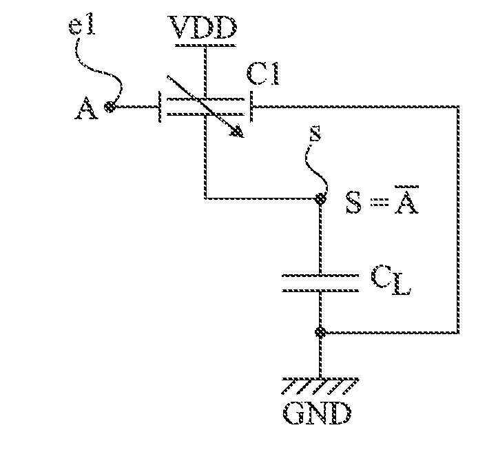
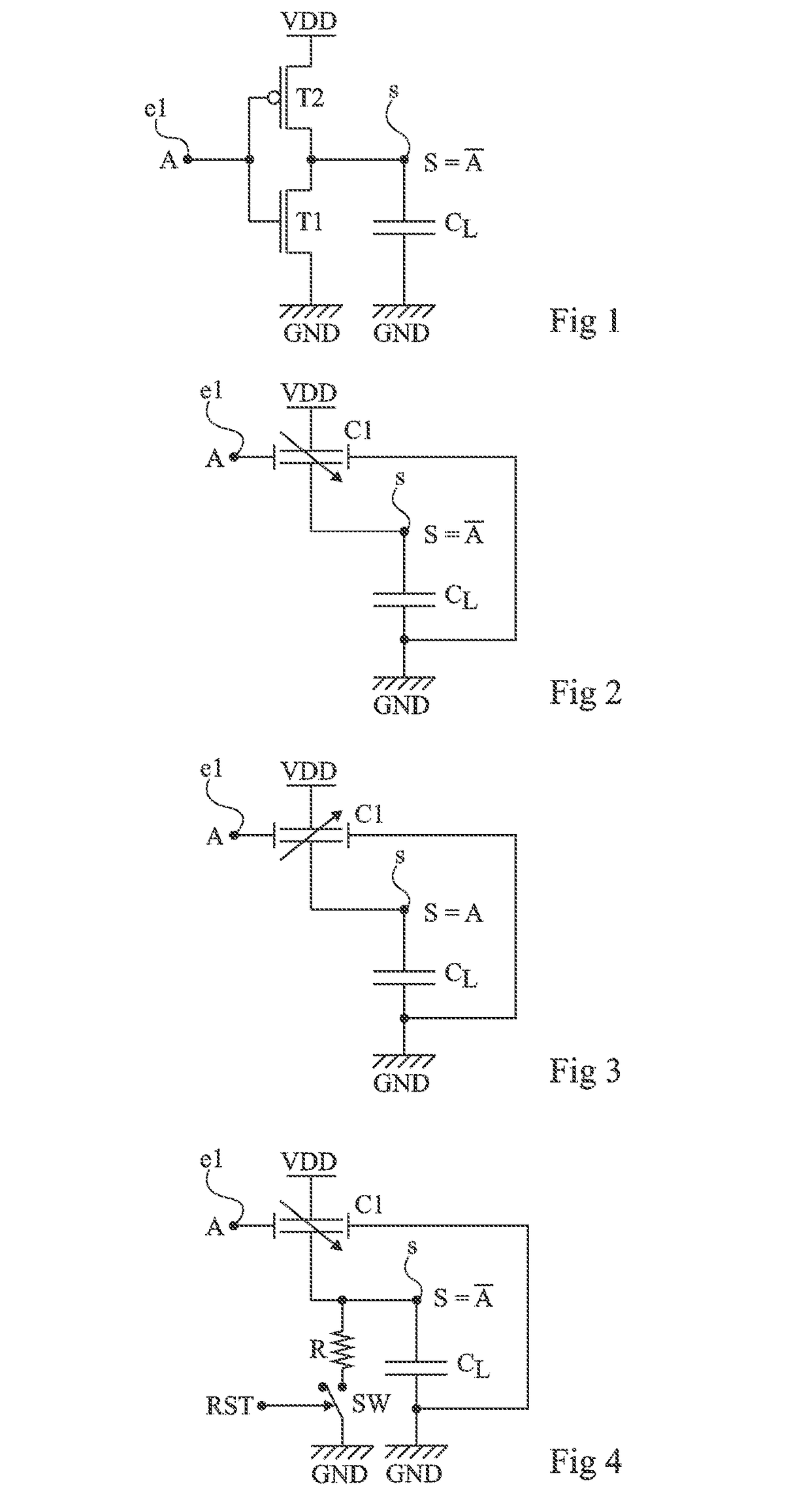
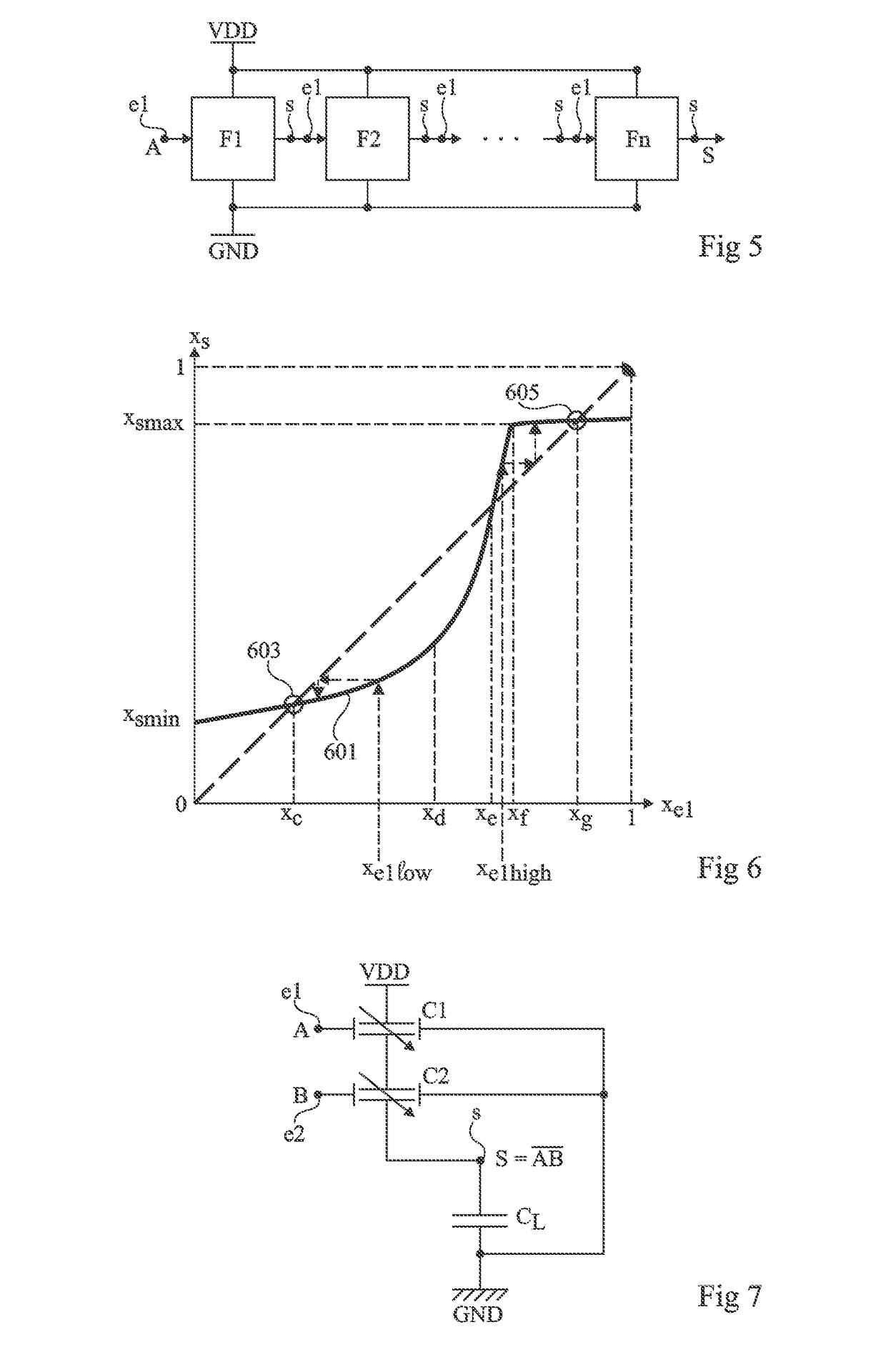
[0057]FIG. 2 is an electric diagram of an example of a logic cell according to the first embodiment. The cell of FIG. 2 is an inverting cell. This cell comprises a variable-capacitance capacitor C1 having two main electrodes separated by an insulating region, for example, a dielectric layer, and two control electrodes electrically insulated from the main electrodes and capable of receiving a control voltage to vary the capacitance between the main electrodes. Embodiments of such capacitors will be described in further detail hereafter in relation with FIGS. 16A, 16B, 17A, 17B and 18. In the example, capacitor C1 is a capacitor having a negative capacitance variation, that is, the capacitance of capacitor C1 takes a low valu...

second embodiment

[0087]FIG. 12 is an electric diagram of an example of a buffer-type adiabatic logic cell according to the The cell of FIG. 12 comprises the same elements as the buffer cell of FIG. 3, arranged substantially in the same way, but differs from the cell of FIG. 3 in that, in the cell of FIG. 12, DC power supply voltage VDD of the cell of FIG. 3 is replaced with a periodic variable power supply voltage Φ(t), supplied by a variable voltage source, not shown. Further, the cell of FIG. 12 comprises a hold and reset circuit comprising a variable-capacitance capacitor Cm, for example, identical to capacitor C1, having its main electrodes respectively connected to the node of application of power supply voltage Φ(t) and to output node s of the cell, and having its control electrodes respectively connected to output node s of the cell and to node GND.

[0088]FIG. 13 is a diagram illustrating the operation of the cell of FIG. 12. More particularly, FIG. 13 illustrates the time variation of power ...


PUM


Abstract

The invention relates to a logic cell for an integrated circuit including at least one first variable-capacitance capacitor having first and second main electrodes separated by an insulating region, and a third control electrode capable of receiving a control voltage referenced to a reference node of the cell to vary the capacitance between the first and second main electrodes, the third electrode being coupled to a node of application of a first logic input signal of the cell, and the first and second electrodes being respectively coupled to a node of application of a cell power supply voltage and to a node for supplying a logic output signal of the cell.

Description

CROSS-REFERENCE TO RELATED APPLICATIONS[0001]This application claims priority to French patent application number 15 / 62812, filed Dec. 18, 2015, which is hereby incorporated by reference in its entirety to the maximum extent allowable by law.BACKGROUND[0002]The present application relates to the field of integrated circuits comprising cells implementing logic functions, also called logic cells or logic gates. The present disclosure more particularly aims at low-consumption logic cells, and at an integrated circuit comprising such logic cells.DISCUSSION OF THE RELATED ART[0003]Logic circuits of the state of the art are generally formed from field-effect transistors, for example, in CMOS (“Complementary Metal-Oxide Semiconductor”) technology, which associates two complementary MOS transistors, one of type N, the other one of type P, on a same support.[0004]FIG. 1 is an electric diagram of an example of an inverting logic cell, that is, a cell carrying out the NO basic function, in CMO...

Claims


Application Information

Patent Timeline
IPC IPC(8): H03K19/00H03K19/185
CPCH03K19/0008H03K19/02H03K19/0013H03K19/185H03K19/0019H03K19/20
Inventor FANET, HERVEHOURI, SAMERPILLONNET, GAEL
Owner COMMISSARIAT A LENERGIE ATOMIQUE ET AUX ENERGIES ALTERNATIVES
Learn More