
Light emitting diode package structure

a technology of light-emitting diodes and package structures, applied in the field of package structures, can solve the problems that the amount of molding compound used cannot be decreased, and the led package structure cannot meet the thinning demand of today, and achieve the effect of improving structural reliability and thinning the package thickness

Inactive Publication Date: 2017-03-02
GENESIS PHOTONICS INC
View PDF4 Cites 3 Cited by
  • Summary
  • Abstract
  • Description
  • Claims
  • Application Information

AI Technical Summary

Benefits of technology

The solution results in a thinner package thickness and improved structural reliability by eliminating the need for wire bonding and minimizing thermal expansion-induced peeling, while maintaining effective LED fixation and light emission efficiency.

Problems solved by technology

However, a height of the bonding wire required by the wire bonding may directly influence a usage amount of a molding compound and an overall thickness of the LED package structure, so that the usage amount of the molding compound cannot be decreased, and the LED package structure cannot satisfy today's thinning demand.

Method used


Image

  • Light emitting diode package structure
  • Light emitting diode package structure
  • Light emitting diode package structure

Examples


Embodiment Construction

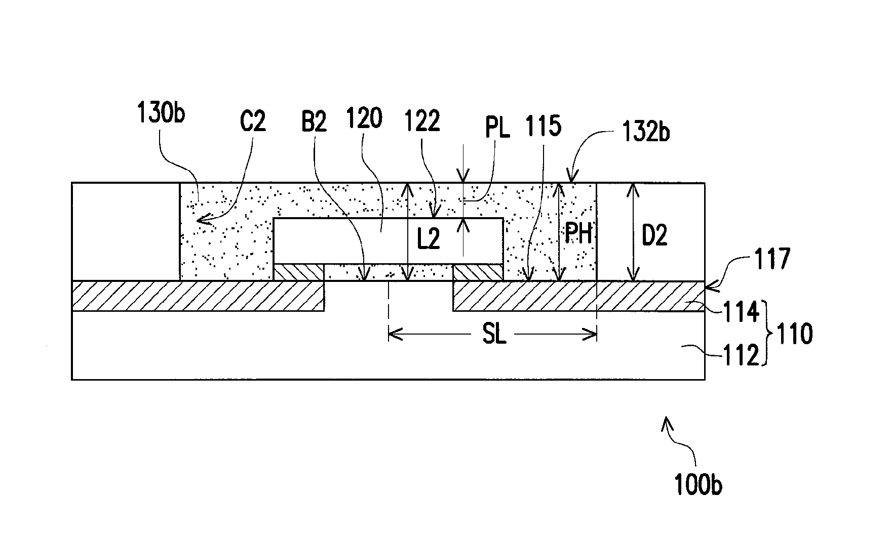
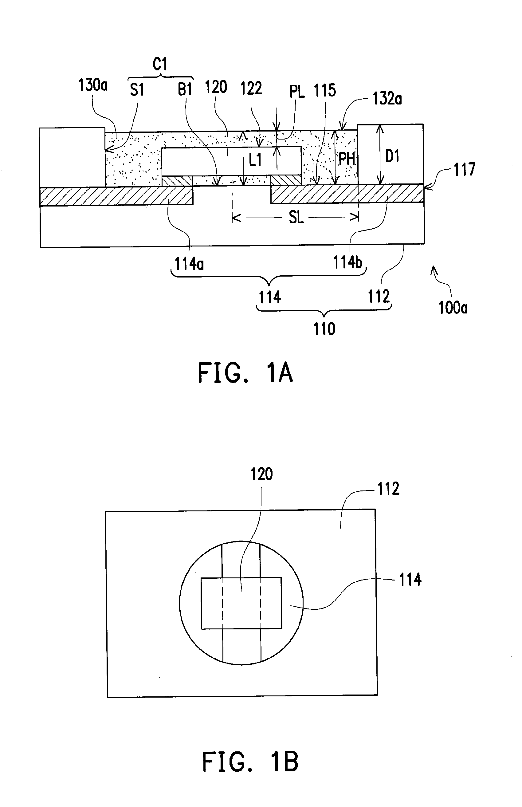
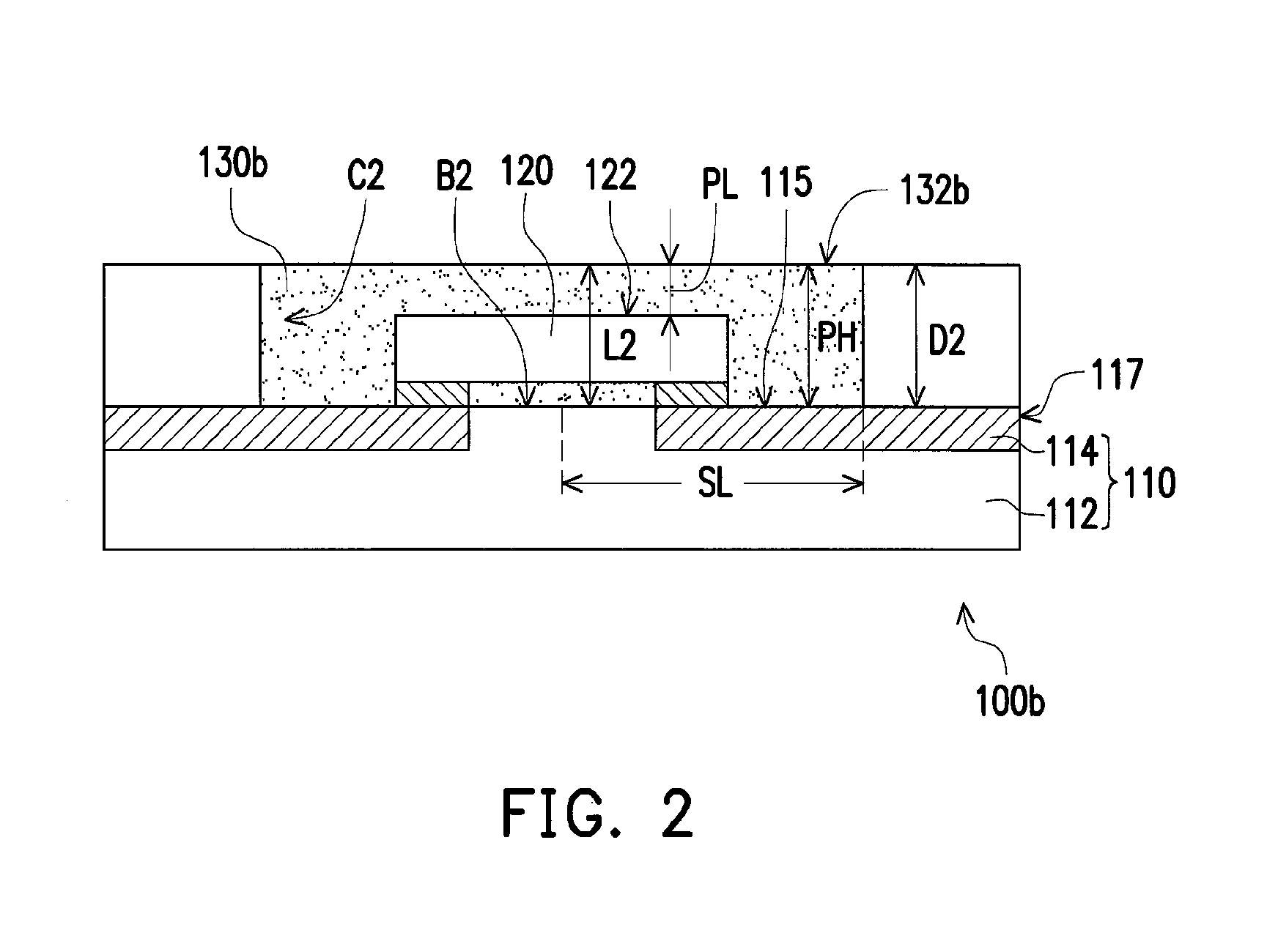
[0025]FIG. 1A is a cross-sectional view of a light emitting diode (LED) package structure according to an embodiment of the invention. FIG. 1B is a top view of the LED package structure of FIG. 1A. Referring to FIG. 1A, in the present embodiment, the LED package structure 100a includes a carrier substrate 110, a flip-chip LED 120 and a molding compound 130a. The carrier substrate 110 includes a main body 112 and a patterned conductive layer 114 embedded in the main body 112. The main body 112 is composed of a polymer material. The main body 112 has a cavity C1, and a bottom surface B of the cavity C1 is aligned with an upper surface 115 of the patterned conductive layer 114. A difference in coefficient of thermal expansion (CTE) between the main body 112 in a rubbery state and the patterned conductive layer 114 is smaller than 30 ppm / ° C. The flip-chip LED 120 is disposed inside the cavity C1 of the carrier substrate 110 and straddles the patterned conductive layer 114. The molding ...


PUM


Abstract

A LED package structure including a carrier substrate, a flip-chip LED and a molding compound is provided. The carrier substrate includes a main body and a patterned conductive layer embedded in the main body. The main body is composed of polymer material. The main body has a cavity, and a bottom surface of the cavity is aligned with an upper surface of the patterned conductive layer. A difference in coefficient of thermal expansion between the main body in a rubbery state and the patterned conductive layer is smaller than 30 ppm / ° C. The flip-chip LED is disposed inside the cavity and electrically connected to the patterned conductive layer. The molding compound is disposed inside the cavity and encapsulates the flip-chip LED. A vertical distance between a top surface of the molding compound and the bottom surface of the cavity is smaller than or equal to a depth of the cavity.

Description

CROSS-REFERENCE TO RELATED APPLICATION[0001]This application is a divisional application of U.S. application Ser. No. 14 / 686,790, filed on Apr. 15, 2015, now allowed. The prior application Ser. No. 14 / 686,790 claims the priority benefit of Taiwan application serial no. 103116264, filed on May 7, 2014. The entirety of each of the above-mentioned patent application is hereby incorporated by reference herein and made a part of this specification.BACKGROUND OF THE INVENTION[0002]Field of the Invention[0003]The invention relates to a package structure, and particularly relates to a light emitting diode package structure.[0004]Description of Related Art[0005]In a conventional concave cup type light emitting diode (LED) package structure, a LED is generally disposed on a main body of a carrier substrate made of a ceramic material, where the LED is located in a cavity and is electrically connected to a pin electrode of the carrier substrate through wire bonding. However, a height of the bon...

Claims


Application Information

Patent Timeline
Patent Type & Authority Applications(United States)
IPC IPC(8): H01L33/48H01L33/50H01L33/54H01L33/62
CPCH01L33/486H01L33/62H01L33/56H01L33/502H01L33/54H01L33/507H01L2224/16H01L2924/181H01L2924/00012
Inventor LIN, YU-FENGKUO, PO-TSUNTSAI, MENG-TING
Owner GENESIS PHOTONICS INC
Learn More