Chip packaging structure and manufacturing method thereof

A technology of chip packaging structure and manufacturing method, which is applied in semiconductor/solid-state device manufacturing, electrical components, electric solid-state devices, etc., can solve the problems of thicker packaging structure and high process cost, and achieve manufacturing cost saving, small integrated body and effect of weight

Pending Publication Date: 2021-07-30
何崇文
View PDF0 Cites 0 Cited by
  • Summary
  • Abstract
  • Description
  • Claims
  • Application Information

AI Technical Summary

Problems solved by technology

In the conventional technology, usually after the packaging is completed, a metal coating is formed on the outside of the packaging colloid by electroplating or sputtering to improve the EMI shielding performance of the packaging structure, but this will increase the thickness of the packaging structure. And the process cost is also higher

Method used


Image

  • Chip packaging structure and manufacturing method thereof
  • Chip packaging structure and manufacturing method thereof
  • Chip packaging structure and manufacturing method thereof

Examples


Embodiment Construction

[0076] Reference will now be made in detail to the exemplary embodiments of the present invention, examples of which are illustrated in the accompanying drawings. Wherever possible, the same reference numbers are used in the drawings and descriptions to refer to the same or like parts.

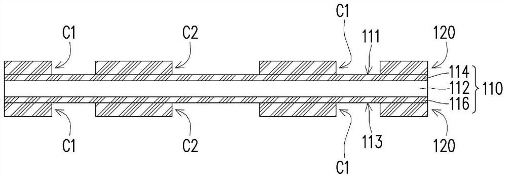
[0077] Figure 1A to Figure 1J It is a schematic cross-sectional view of a manufacturing method of a chip packaging structure according to an embodiment of the present invention. Regarding the manufacturing method of the chip packaging structure of this embodiment, first of all, please refer to Figure 1F , providing the carrier 100 formed with a plurality of conductive blocks 210 and at least one metal layer 220 (two metal layers 220 are schematically shown). For details, please refer to Figure 1A , providing a substrate 110 , wherein the substrate 110 includes a core layer 112 , a first conductive layer 114 and a second conductive layer 116 . The first conductive layer 114 and the second...


PUM


Abstract

The invention provides a chip packaging structure and a manufacturing method thereof. The manufacturing method of the chip packaging structure comprises the following steps that: a carrier plate on which a plurality of conductive blocks and at least one metal layer have been formed is provided, the carrier plate comprises a base material and a stainless steel layer sputtered on the base material, the base material is provided with a plurality of first grooves and at least one second groove surrounding the first grooves, the stainless steel layer conformally covers the first grooves and the second grooves to define a plurality of third grooves and at least one fourth groove, the third grooves are filled with the conductive blocks, the metal layer covers the stainless steel layer, the conductive blocks and the fourth grooves to define at least one fifth groove; at least one chip is arranged in the fifth groove; at least one circuit structure layer is formed on the carrier plate; the patterned circuit layer of the circuit structure layer is electrically connected with the plurality of electrodes of the chip; and the carrier plate and the circuit structure layer are separated to expose the conductive blocks and the metal layer.

Description

technical field [0001] The present invention relates to a packaging structure and a manufacturing method thereof, and in particular to a chip packaging structure and a manufacturing method thereof. Background technique [0002] In the well-known coreless process, the edge of the partial carrier board and the edge of the partial circuit board are first bonded by adhesive glue or copper-plated edge sealing. Another conventional method is to use a thin substrate (thickness, for example, 100 microns) containing glass fiber cloth, and each side is followed by a piece of copper foil and a peelable ultra-thin copper foil (thickness, for example, 3 microns) attached to it. microns to 5 microns) as a carrier. After the circuit board has gone through multiple processes, the portion with adhesive or copper-plated edge sealing between the carrier board and the circuit board is cut off to obtain a circuit board for the packaging process. However, in the known coreless process, part of ...

Claims


Application Information

Patent Timeline
IPC IPC(8): H01L23/31H01L23/498H01L23/48H01L21/56
CPCH01L21/561H01L23/3121H01L23/481H01L23/49838
Inventor 何崇文
Owner 何崇文
Why Eureka
Try Eureka