Semiconductor technology and the silicon substrate and chip packaging structure formed by applying this technology

A semiconductor and process technology, which is applied in the field of silicon substrate and chip packaging structure, can solve problems such as inability to achieve thinning, and achieve the effect of thin package thickness

Inactive Publication Date: 2011-12-07
UNIMICRON TECH CORP
View PDF5 Cites 0 Cited by
  • Summary
  • Abstract
  • Description
  • Claims
  • Application Information

AI Technical Summary

Problems solved by technology

However, the overall height of the ball grid array (BGA) package structure is about 1.0-1.4mm, which cannot meet the requirement of thinning (less than 0.5mm)

Method used


Image

  • Semiconductor technology and the silicon substrate and chip packaging structure formed by applying this technology
  • Semiconductor technology and the silicon substrate and chip packaging structure formed by applying this technology
  • Semiconductor technology and the silicon substrate and chip packaging structure formed by applying this technology

Examples


Embodiment Construction

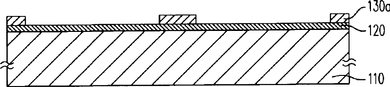
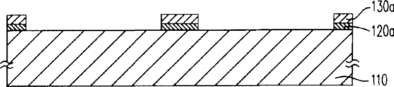
[0038] Please refer to Figure 1B , and then, forming a first patterned photoresist mask 130 a on the first insulating layer 120 . Next, at least one stepped structure 140 is formed on the silicon substrate 110 (please refer to Figure 1L ). In detail, the steps of forming the stepped structure 140 are as follows, please refer to Figure 1C and Figure 1D , first, using the first patterned photoresist mask 130a as an etching mask, etch the first insulating layer 120 exposed outside the first patterned photoresist mask 130a to form a patterned The first insulating layer 120a. Next, the first patterned photoresist mask 130a is removed to expose the patterned first insulating layer 120a under the first patterned photoresist mask 130a. Please refer to Figure 1E , and then, using the patterned first insulating layer 120a as an etching mask, etching the silicon substrate 110 exposed outside the patterned first insulating layer 120a to form at least one layer having a first de...


PUM

PropertyMeasurementUnit
heightaaaaaaaaaa

Abstract

The invention provides a semiconductor process and a silicon substrate and a chip packaging structure formed by applying the process. First, a silicon substrate is provided. Next, a surface of the silicon substrate is partially exposed, and the surface of the silicon substrate is etched, so that the silicon substrate is formed with at least one stepped shape with a first notch having a first depth and a second notch having a second depth structure. The first depth is smaller than the second depth, and the aperture of the first notch is larger than the aperture of the second notch. A final insulating layer, a metal seed layer and a ladder-like structure are sequentially formed. A patterned photoresist layer is formed on the metal seed layer. A circuit layer is formed to cover part of the metal seed layer exposed above the first notch. Afterwards, the patterned photoresist layer and part of the metal seed layer under it are removed.

Description

technical field [0001] The present invention relates to a semiconductor process, and in particular to a silicon substrate and a chip packaging structure formed by applying the semiconductor process. Background technique [0002] Nowadays, with advanced semiconductor technology, an integrated circuit chip (IC chip) has a large number of transistors arranged in high density and many signal pads arranged on the surface of the chip. In order to package these chips, these chips are usually mounted on a chip package substrate to form a chip package structure, wherein the chip can obtain sufficient signal paths, heat dissipation paths and structural protection through the packaging process. [0003] At present, with the continuous improvement of packaging technology, various chip packaging structures are constantly being introduced. For example, the chip is attached to the chip pad or the inner pin of the lead frame to form a thin small size package (TSOP), Alternatively, the chip...

Claims


Application Information

Patent Timeline
Patent Type & Authority Patents(China)
IPC IPC(8): H01L21/48H01L21/50H01L23/488H01L23/31
CPCH01L24/97H01L2224/48091H01L2224/49171H01L2924/14H01L2924/15787H01L2924/18165
Inventor 吕致纬
Owner UNIMICRON TECH CORP
Why Eureka
Try Eureka