Multiple conductive layer TFT

a thin film transistor and multi-layer technology, applied in the direction of semiconductor devices, semiconductor/solid-state device details, electrical equipment, etc., can solve the problems of high capital equipment, materials and manufacturing costs, and difficulty in fabricating metallic interconnect lines with a width of less than 50-100 m, so as to reduce the change of debris-induced electrical shorts between electrodes and achieve high accuracy alignment

Active Publication Date: 2016-12-29
FLEXENABLE TECH LTD
View PDF3 Cites 0 Cited by
  • Summary
  • Abstract
  • Description
  • Claims
  • Application Information

AI Technical Summary

Benefits of technology

The invention relates to a structure for a thin film transistor (TFT) and a storage capacitor in a display device. By separating the gate electrode of the TFT from the first plate of the capacitor, the structure provides better alignment tolerance for the different layers in the device. This allows for independent optimization of different dielectric materials for the gate interconnect line and the storage capacitor, resulting in better pixel capacitance values, and reduces the risk of electrical shorts between electrodes caused by debris. This is particularly useful for high resolution active matrices.

Problems solved by technology

Silicon based processes require a combination of vacuum deposition and subtractive photolithographic patterning steps leading to high capital equipment, materials and manufacturing costs.
However, when using printing processes such as inkjet printing, screen printing and offset printing, it is difficult to fabricate metallic interconnect lines with a width of less than 50-100 μm because of the difficulties associated with delivering small volumes of liquid.
However, even using this technique, achieving linewidths of less than 10-20 μm can be challenging.
Furthermore, many printable conductors such as conducting polymers or colloidal metals have conductivities significantly lower than bulk copper or silver, therefore requiring thick and wide interconnect lines to achieve adequate conductance across a large active matrix.
In a conventional pixel architecture for an active matrix application, where the data line, the source and drain electrode of the TFT, the pixel electrode and the pixel capacitor are all defined in the same layer of the device, and compete with each other for space, the limited printing resolution reduces the achievable aperture ratio and front-of-screen performance of the display.
The areas of the gate interconnect lines and the capacitor counter electrode needs to be shielded from the viewer, as the electrical signals on these lines induce undesirable optical contrast of the display element.
In a transmissive display the aperture ratio restrictions are even harder to counteract.
This is caused by the fact that most inorganic metallic conductors, with the exception of indium tin oxide, are not sufficiently transparent.
This would not be possible for structures that incorporate all of the elements of a transistor, such as a source and drain electrodes, source data line and a pixel capacitor on the same metal level as the pixel electrode.
However, it is important not to increase this storage capacitance at the expense of the switchable area and the resulting aperture ratio.
However, it is often a problem within the prior art that the size of the capacitor structure is limited as it competes for space within the device, with the TFT structure and the via pad.
When using printing processes such as inkjet printing, screen printing and offset printing, it is difficult to fabricate metallic interconnect lines with a width of less than 50-100 μm because of the difficulties associated with delivering small volumes of liquid.
However, even using this technique, achieving linewidths of less than 10-20 μm can be challenging.
Furthermore, many printable conductors such as conducting polymers or colloidal metals have conductivities significantly lower than bulk copper or silver, therefore requiring thick and wide interconnect lines to achieve adequate conductance across a large active matrix.
Therefore, by using conventional display architectures, printed electrode and printed pixel capacitors tend to be large and result in active matrix displays with low aperture ratios.

Method used


Image

  • Multiple conductive layer TFT
  • Multiple conductive layer TFT
  • Multiple conductive layer TFT

Examples


first embodiment

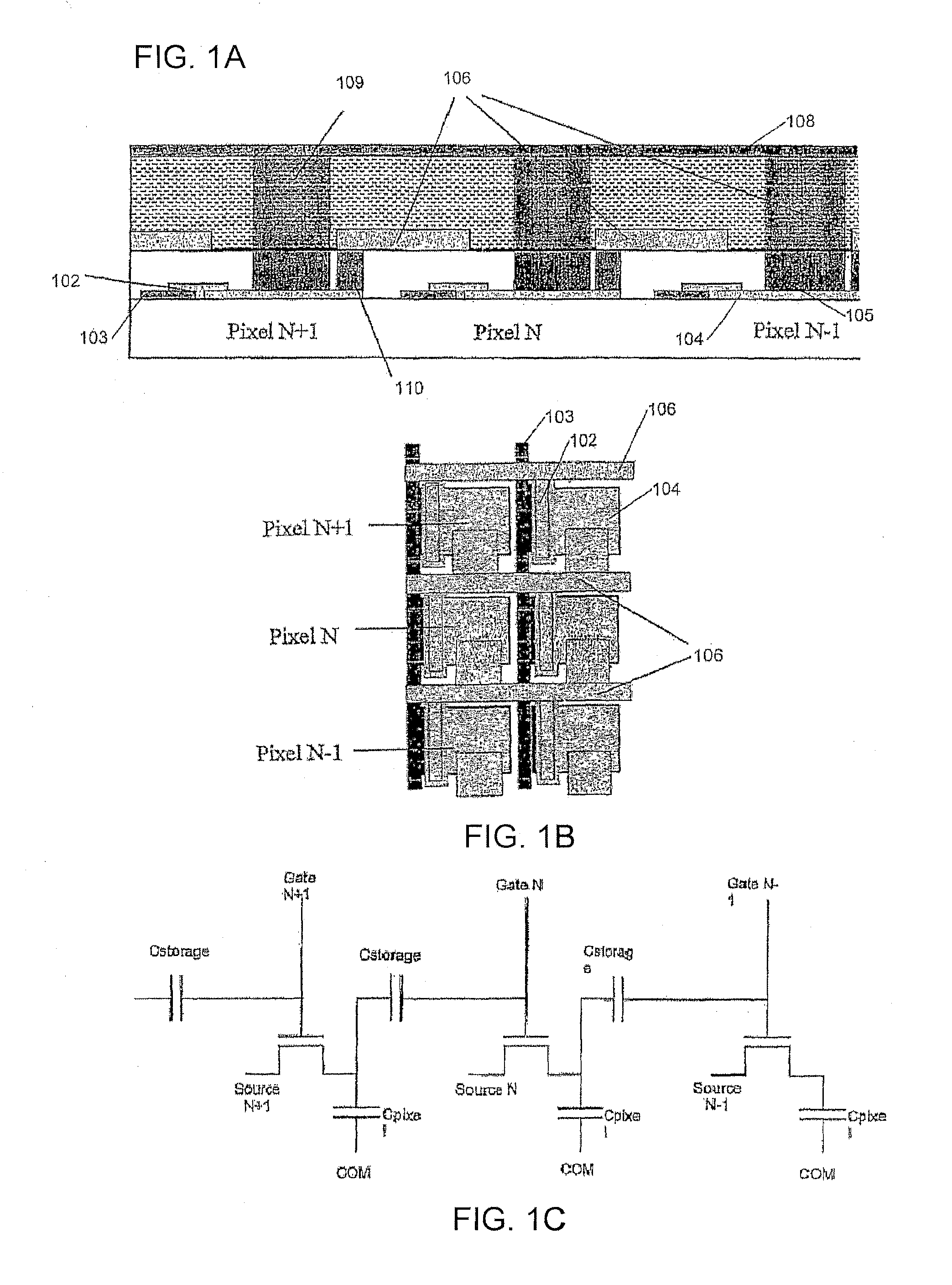
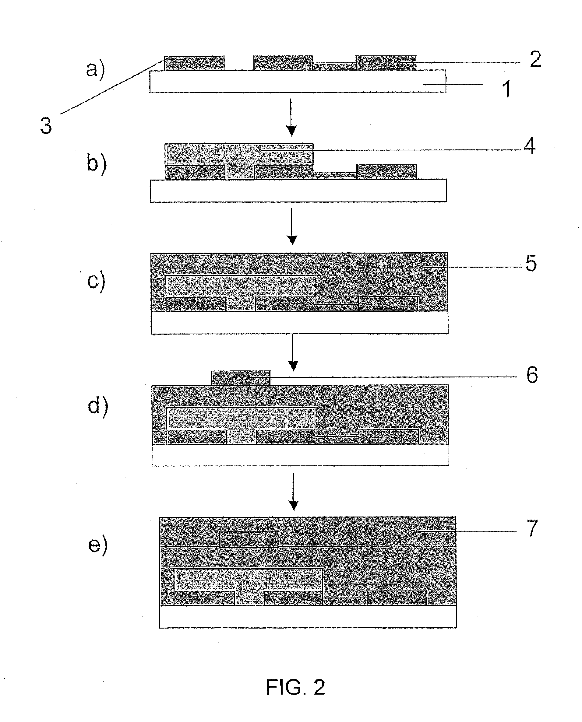
[0061]With reference to FIGS. 2 and 3A-3E, the present invention is now described in detail. A substrate 1 is coated with a thin layer of conductive material. The substrate may be either glass or a polymer film. According to a preferred embodiment of the invention the substrate is a plastic substrate, such as a film of polyethyleneterephtalate (PET) or polyethylenenaphtalene (PEN). A first conductive layer 2, is preferably a metallic layer, and most preferably a layer of inorganic metal such as gold or silver; or any metal that adheres well to the substrate and is electrically compatible with the chosen semi-conductor may also be used, or any combination of metals to achieve these effects. A bilayer structure may be deposited, including a seed or adhesion layer in between the layer of metallic material and the substrate. Alternatively, a conductive polymer may be used, such as PEDOT / PSS. The conductive material is preferably deposited using solution processing techniques such as, bu...

second embodiment

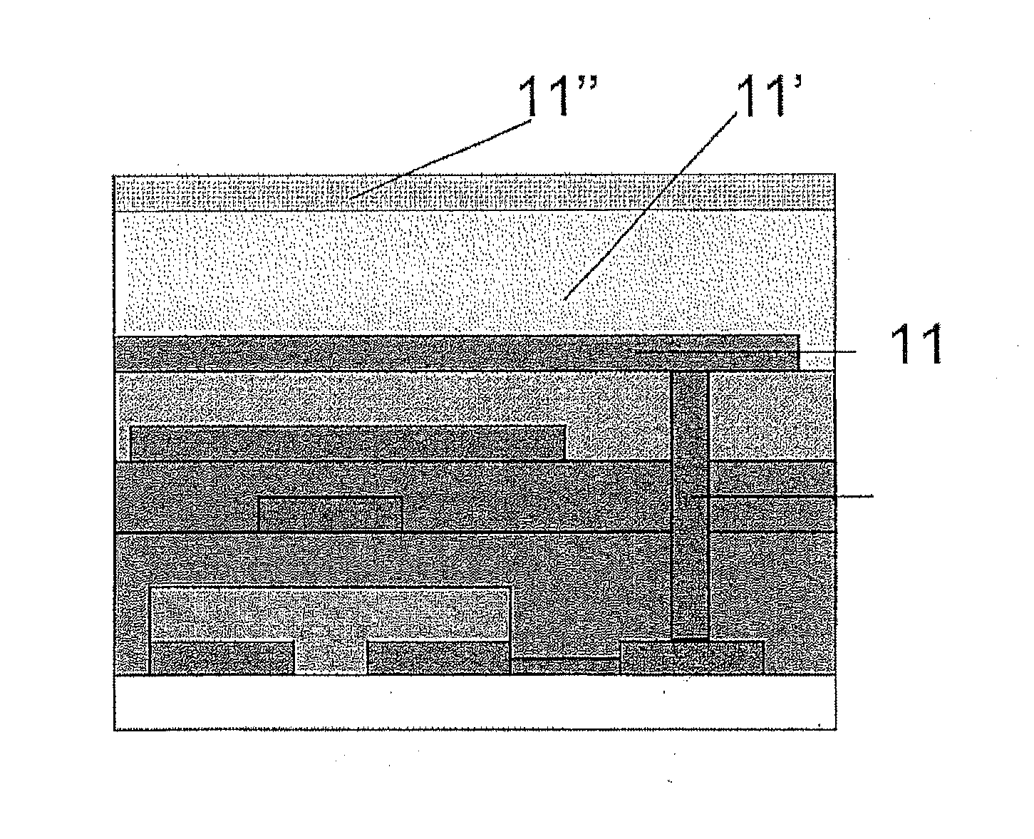
[0075]the present invention provides a five layer transistor device structure as is illustrated in FIGS. 4A-4C. As described above, this structure incorporates an additional conductive layer as a capacitor layer and overlying dielectric material layer which allows a lower tolerance for the dielectric layer deposited above the COM layer, for example for thickness of the layer. The addition of both the dielectric layer above the capacitor level and the layer of dielectric material above the COM layer may be used in a capacitor structure where there is a requirement for the capacitance to be high. This five layer sandwich structure is advantageous as it allows a thicker top dielectric layer to be used and allows the patterning of the top pixel electrode to be achieved more readily and allows the possibility of higher Cstorage values.

[0076]With reference to FIGS. 4A-4C which continues to FIG. 2, a second embodiment of the present invention is now described. As stated above, the material...


PUM

PropertyMeasurementUnit
widthaaaaaaaaaa
wavelengthaaaaaaaaaa
depositionaaaaaaaaaa

Abstract

A multiple layer pixel architecture for an active matrix display is provided having a common bus line on a metal level separate from that on which the gate electrodes of the thin-film transistors (TFTs) are formed. A multilayer electronic structure includes a TFT for driving a pixel of an active matrix optoelectronic device and a capacitor for storing charge to maintain an electrical state of said active matrix pixel, wherein the structure includes a substrate bearing at least four conducting layers separated by at least three dielectric layers, first and second ones of said conducting layers defining drain / source electrodes and a gate electrode of said transistor respectively, and third and fourth ones of said conducting layers defining respective first and second plates of said capacitor, wherein said capacitor and said transistor are laterally positioned such that they overlap in a vertical direction.

Description

CROSS-REFERENCE TO RELATED APPLICATIONS[0001]This application is a divisional of U.S. patent application Ser. No. 11 / 910,733, having a 35 U.S.C. §371(c) date of Jul. 28, 2008, which is the U.S. National Phase under 35 U.S.C. §371 of International Application No. PCT / GB2006 / 050078, filed Apr. 5, 2006, designating the United States and published in English on Oct. 12, 2006, as WO 2006 / 106365, which claims priority to United Kingdom Application No. 0511117.4, filed Jun. 1, 2005 and United Kingdom Application No. 0506899.4, filed Apr. 5, 2005.TECHNICAL FIELD[0002]The present invention relates to a multiple layer thin film transistor (TFT) structure for use for an active matrix polymer TFT display fabricated using techniques such as solution processing and direct printing.DESCRIPTION OF THE RELATED ART[0003]In accordance with the prior art, multi-layer active matrix displays are well known. Conventional thin film transistors (TFT) are typically fabricated with inorganic silicon, such as ...

Claims


Application Information

Patent Timeline
Patent Type & Authority Applications(United States)
IPC IPC(8): H01L27/28H01L51/05H01L51/00H01L51/10H01L23/528H01L27/32
CPCH01L27/283H01L23/5286H01L27/3262H01L27/3265H01L2227/323H01L27/3274H01L51/0022H01L51/105H01L51/0512H01L27/3276H10K59/1216H10K59/1213H10K19/10H10K10/84H10K10/462H10K59/125H10K59/131H10K71/611H10K59/1201
Inventor REYNOLDS, KIERANRAMSDALE, CATHERINEJACOBS, KEVINREEVES, WILLIAM
Owner FLEXENABLE TECH LTD
Why Eureka
Try Eureka