Thin substrate processing device
a technology of processing device and thin substrate, which is applied in the direction of electrolysis components, vacuum evaporation coatings, coatings, etc., can solve the problems of limited temperature rise of thin substrate, and achieve the effect of enhancing the cooling effect of thin substra
- Summary
- Abstract
- Description
- Claims
- Application Information
AI Technical Summary
Benefits of technology
Problems solved by technology
Method used
Image
Examples
first embodiment
[0050]A thin substrate processing device according to a first embodiment will now be described with reference to FIG. 1 to FIG. 12. In the present embodiment, the thin substrate processing device is a sputtering device, for example.
[0051][Entire Configuration of Sputtering Device]
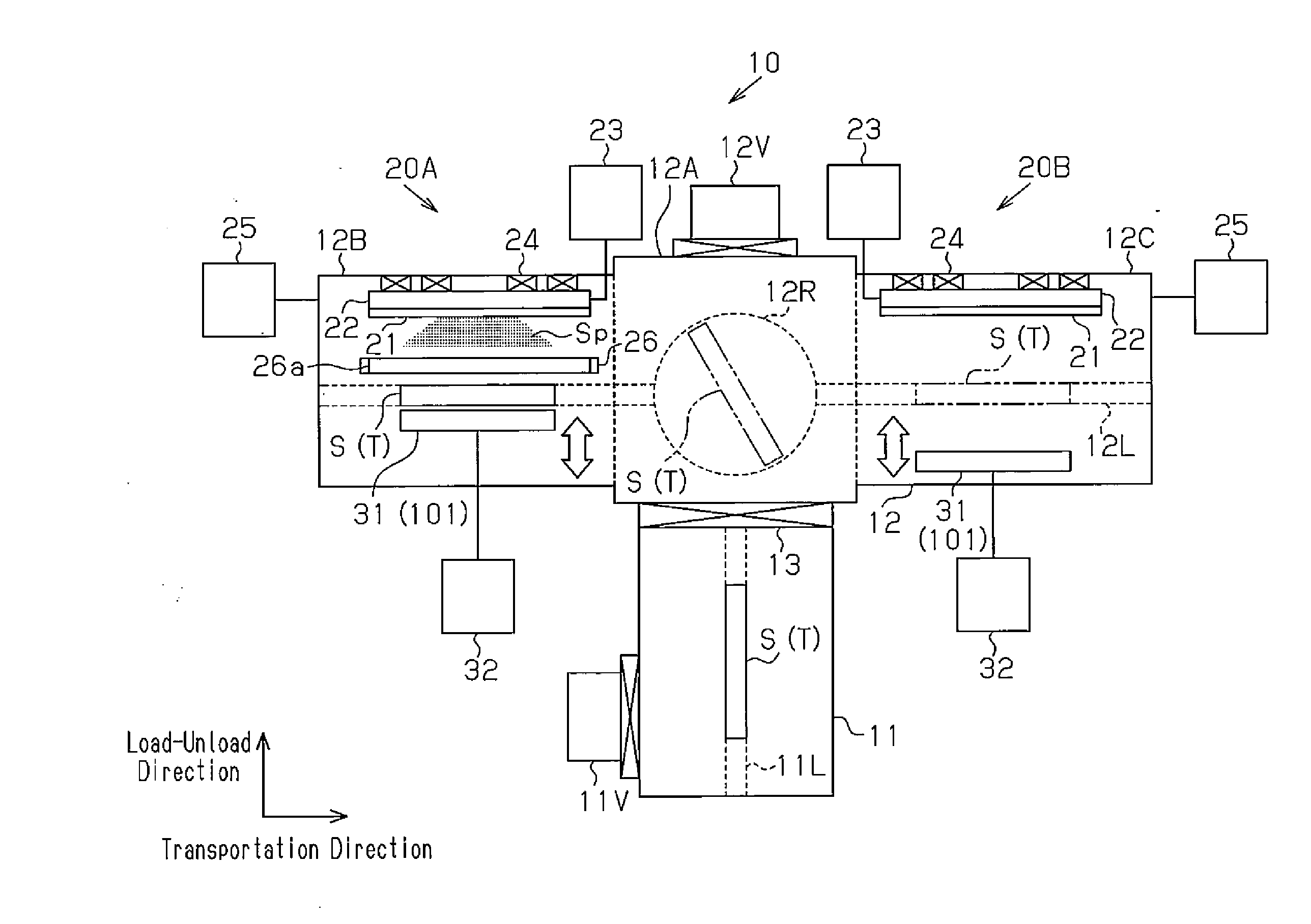
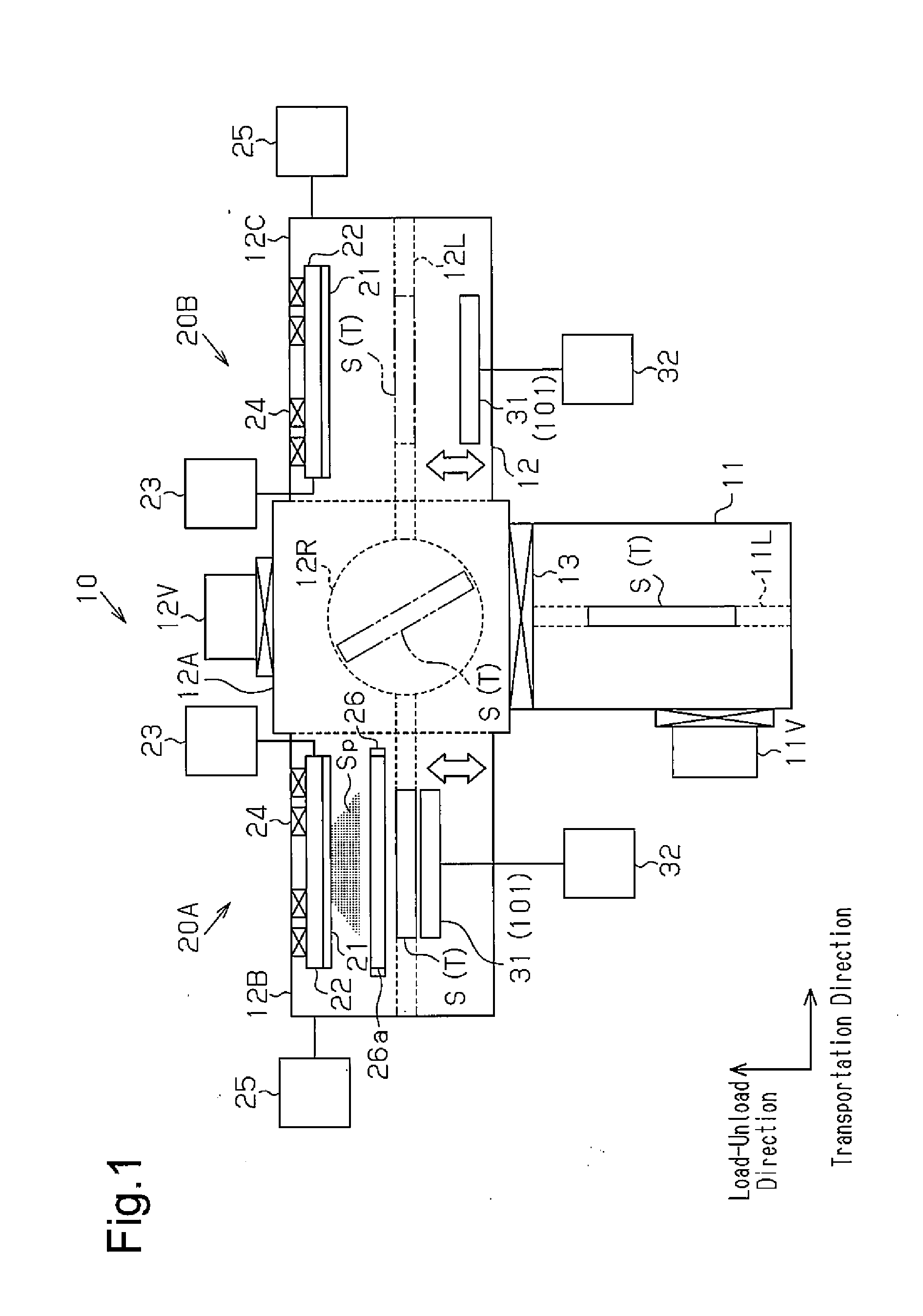
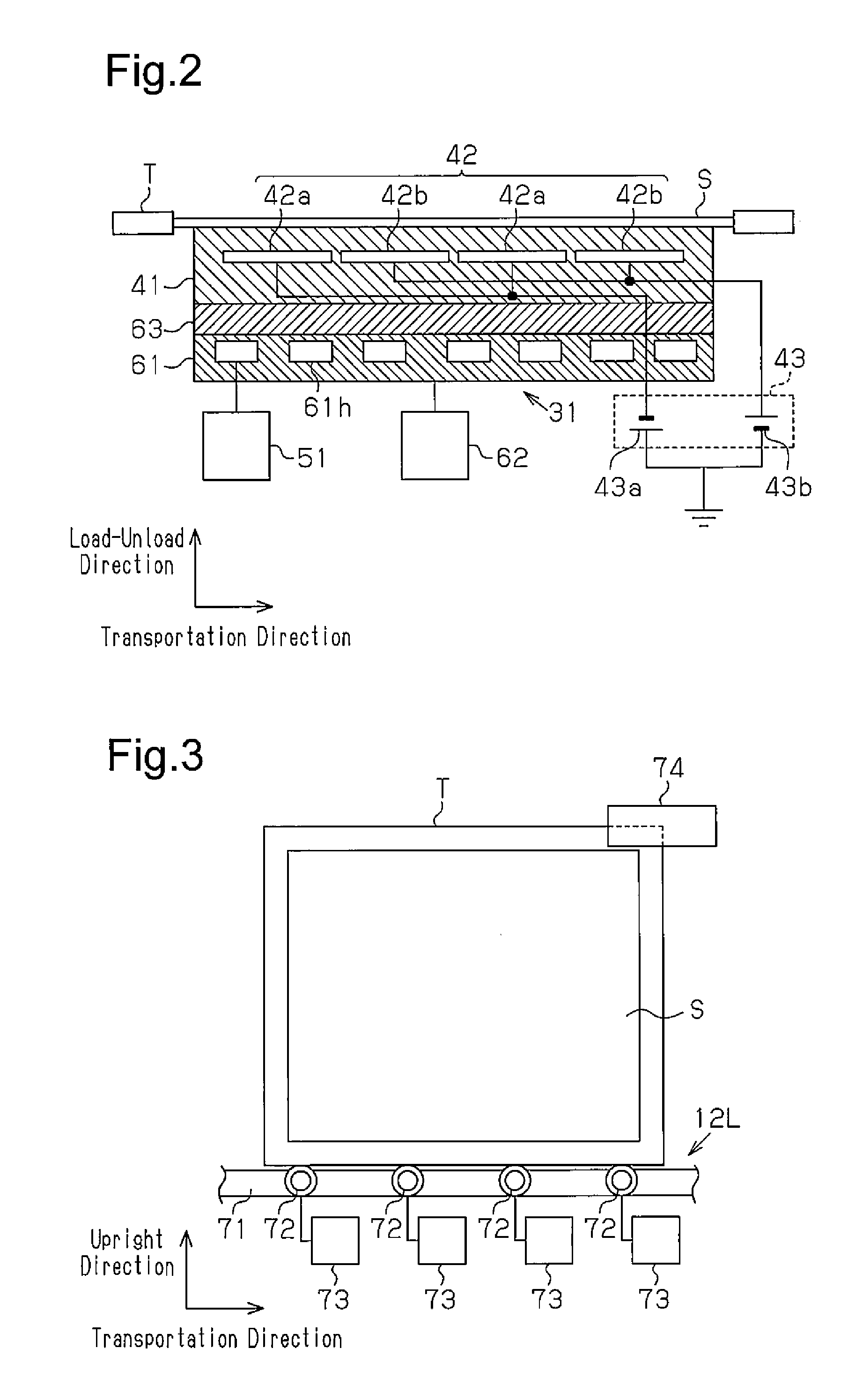
[0052]The entire configuration of a sputtering device 10 will now be described with reference to FIG. 1. As shown in FIG. 1, the sputtering device 10 includes a load-unload chamber 11 and a vacuum chamber 12. The load-unload chamber 11 and the vacuum chamber 12 are formed in box shapes, for example. Between the load-unload chamber 11 and the vacuum chamber 12, a gate valve 13 connects or disconnects the load-unload chamber 11 and the vacuum chamber 12. The load-unload chamber 11 loads and unloads a film substrate S as an example of a thin substrate along a load-unload direction shown in FIG. 1. The vacuum chamber 12 transports the film substrate S along a transportation direction shown in FIG. 1. The load-u...
example 1
[0119]After preparing a printed circuit board and a film substrate made of polyester resin, when forming a copper film on the printed circuit board and the film substrate, the voltage supplied to the chuck electrode of the electrostatic chuck was changed between the printed circuit board and the film substrate. Then, temperatures of the printed circuit board and the film substrate when forming the copper film at each voltage were measured. FIG. 10 shows the measurement result. In FIG. 10, the vertical axis shows a substrate temperature, and the horizontal axis shows the voltage (an absolute value) applied to the chuck electrode.
[0120]The printed circuit board was a substrate obtained by stacking a copper film and a glass epoxy resin layer on a glass epoxy substrate obtained by forming a copper foil on both surfaces of a film obtained by fixing a glass cloth (a core material) with the epoxy resin. A thickness of the printed circuit board was 80 μm, and a thickness of the film substra...
example 2
[0129]After reverse sputtering was performed on the surface of the insulation substrate made of glass epoxy resin, reverse sputtering speeds were measured at different positions with an effective range of the reverse sputtering of the insulation substrate. The size of the effective range of the reverse sputtering was 500 mm×600 mm, and the reverse sputtering was performed under the following condition. Reverse sputtering speeds were measured at two corners (first corner and second corner) located on a diagonal line in the effective range of the reverse sputtering, a central portion, and between each corner and the central portion. FIG. 11 shows the measurement result.
[0130]substrate: glass epoxy resin substrate
[0131]sputtering gas: argon gas
[0132]flow rate: 200 sccm
[0133]frequency: 2 MHz
[0134]electric power amount: 730 W
[0135]pressure: 2 Pa
[0136]As shown in FIG. 11, the reverse sputtering speed at the central portion of the effective range of the reverse sputtering was 1.9 nm / min, a...
PUM
| Property | Measurement | Unit |
|---|---|---|
| Frequency | aaaaa | aaaaa |
| Frequency | aaaaa | aaaaa |
| Frequency | aaaaa | aaaaa |
Abstract
Description
Claims
Application Information
 - R&D
- Intellectual Property
- Life Sciences
- Materials
- Tech Scout
- Unparalleled Data Quality
- Higher Quality Content
- 60% Fewer Hallucinations
Browse by: Latest US Patents, China's latest patents, Technical Efficacy Thesaurus, Application Domain, Technology Topic, Popular Technical Reports.
© 2025 PatSnap. All rights reserved.Legal|Privacy policy|Modern Slavery Act Transparency Statement|Sitemap|About US| Contact US: help@patsnap.com


