
Complementary bipolar SRAM

a bipolar sram and sram technology, applied in the field of transistor devices, can solve the problems of cost-effective building of sram, and achieve the effect of avoiding bicmos processes

Inactive Publication Date: 2016-11-24
INT BUSINESS MASCH CORP
View PDF7 Cites 0 Cited by
  • Summary
  • Abstract
  • Description
  • Claims
  • Application Information

AI Technical Summary

Benefits of technology

The present patent describes a type of memory element called a complementary Bipolar SRAM memory element. This element uses cross-coupled bipolar inverters as the memory cells, and NPN bipolar junction transistors as access devices. This design helps avoid the use of BiCMOS processes and requires only a complementary bipolar device manufacturing process. The technical effect of this design is improved cost efficiency and manufacturing flexibility.

Problems solved by technology

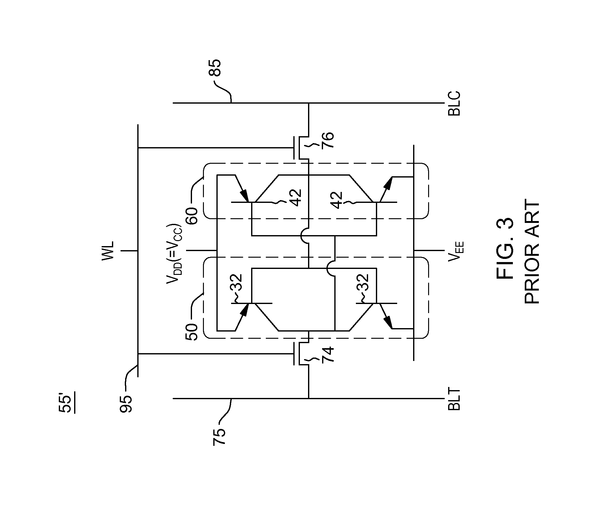
The memory cell 55′ according to prior art implementation of FIG. 3 requires a BiCMOS process, i.e. a manufacturing process that integrates both SOI lateral bipolar inverters and MOSFETs on the same substrate, to build the SRAM which, as known, is not cost-effective.

Method used


Image

  • Complementary bipolar SRAM
  • Complementary bipolar SRAM
  • Complementary bipolar SRAM

Examples


Embodiment Construction

[0028]Aspects of the present disclosure are now described in detail with accompanying figures. It is noted that like reference numerals refer to like elements across different embodiments. The drawings are not necessarily drawn to scale. As used herein, ordinals such as “first,”“second,” and “third,” etc. are employed to distinguish similar elements, and a same element may be labeled with different ordinals across the specification and the claims.

[0029]The present disclosure is directed to a Complementary Bipolar SRAM that avoids BiCMOS processing.

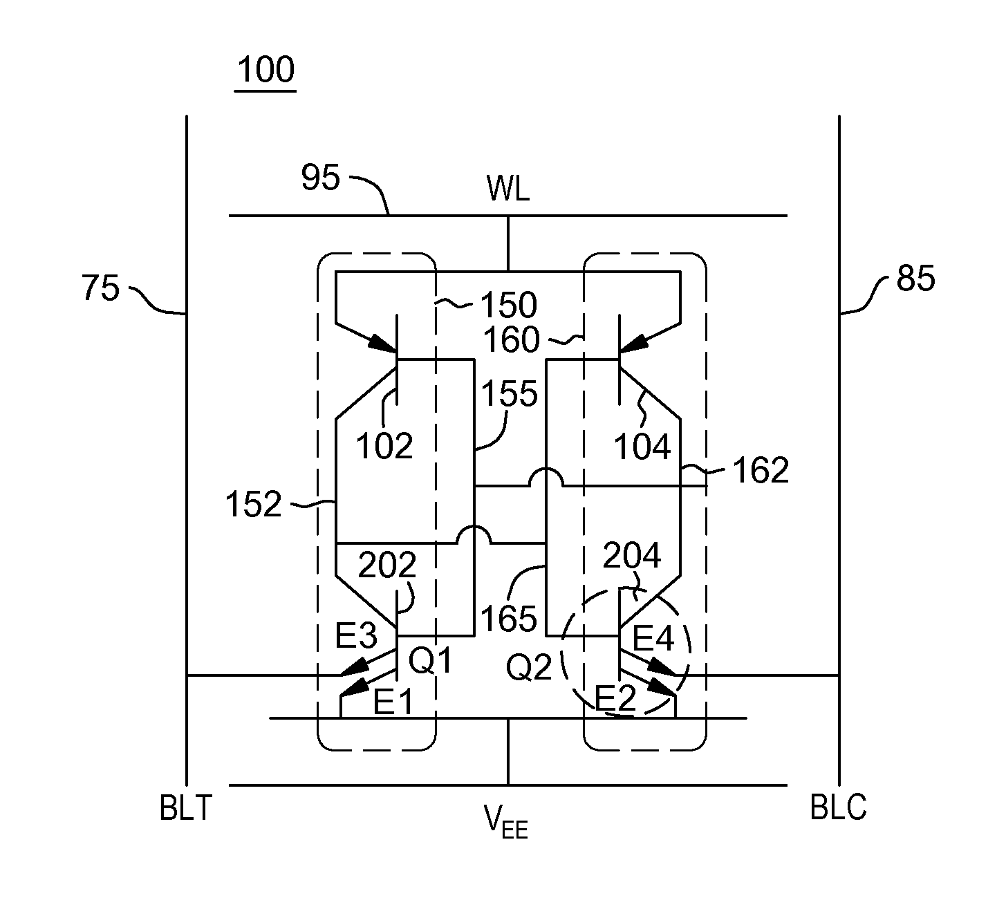
[0030]The current invention is an all bipolar SRAM cell, using cross-coupled complementary semiconductor-on-insulator (SOI lateral bipolar transistors as SRAM memory element, and NPN bipolar transistors as access transistors. No BiCMOS processing is required in its manufacture-only SOI lateral bipolar transistors are formed at a lower cost.

[0031]FIG. 4 shows an embodiment of the SOI lateral bipolar junction transistor (BJT) memory cell 100...


PUM


Abstract

A complementary lateral bipolar SRAM device and method of operating. The device includes: a first set and second set of lateral bipolar transistors forming a respective first inverter device and second inverter device, the first and second inverter devices being cross-coupled for storing a logic state. In each said first and second set, a first bipolar transistor is an PNP type bipolar transistor, and a second bipolar transistor is an NPN type bipolar transistor, each said NPN type bipolar transistor having a base terminal, a first emitter terminal, a second emitter terminal, and a collector terminal. Emitter terminals of the PNP type transistors of each first and second inverter devices are electrically coupled together and receive a first applied wordline voltage. The first emitter terminals of each said NPN transistors of said first inverter and second inverter devices are electrically coupled together and receive a second applied voltage. The second emitter terminal of one NPN bipolar transistor of said first inverter is electrically coupled to a first bit line conductor, and the second emitter terminal of the NPN bipolar transistor of said second inverter device is electrically coupled to a second bit line.

Description

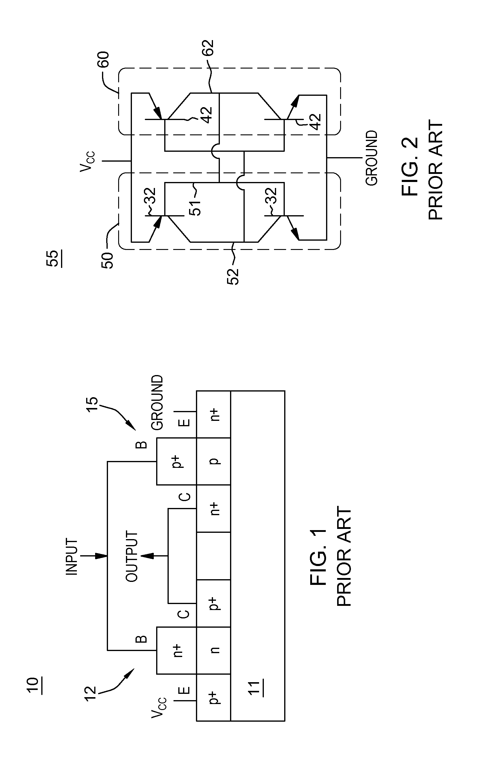
CROSS REFERENCE TO RELATED APPLICATION[0001]This application is a continuation of U.S. patent application Ser. No. 14 / 717,218, filed May 20, 2015 the entire content and disclosure of which is incorporated herein by reference.BACKGROUND[0002]The present invention relates generally to transistor devices, and in particular a complementary bipolar SRAM, and a method of building and operating a complementary bipolar SRAM.[0003]Semiconductor-on-Insulator (SOI) lateral bipolar transistors are ideally suitable for building complementary bipolar inverters, which is the basic building block for complementary bipolar circuits. The teaching of a complementary lateral bipolar inverter using SOI can be found in U.S. Pat. No. 8,531,001.[0004]FIG. 1 shows a SOI lateral bipolar inverter device 10 according to prior art implementations. In FIG. 1 the SOI lateral bipolar junction transistor (BJT) device 10 includes a first bipolar (P-N-P) transistor 12 and a second bipolar (N-P-N) transistor 15 formed...

Claims


Application Information

Patent Timeline
Patent Type & Authority Applications(United States)
IPC IPC(8): G11C11/416H10B10/00
CPCG11C11/416G11C11/4116G11C11/411H10B10/10H10B10/00H01L21/8228
Inventor NING, TAK H.
Owner INT BUSINESS MASCH CORP
Learn More