
Extreme ultra-violet sensitivity reduction using shrink and growth method

a thin film, ultra-violet technology, applied in the direction of microlithography exposure apparatus, instruments, photomechanical treatment, etc., can solve the problems of difficult simultaneous improvement of resolution, lwr, sensitivity, and euv resist sensitivity, and achieve the effect of increasing the substrate throughput of the patterning system

Active Publication Date: 2016-11-17
TOKYO ELECTRON LTD
View PDF4 Cites 303 Cited by
  • Summary
  • Abstract
  • Description
  • Claims
  • Application Information

AI Technical Summary

Benefits of technology

The patent is about a system for making patterns on a substrate using a layer of sensitive material. The system makes the pattern and then shrinks it to a smaller size. The pattern has some roughness, which can be measured as a line edge roughness or a line width roughness. The patent proposes a method to make the pattern so that it is easier to shrink without causing any problems in the pattern. This makes it easier to make the desired pattern and increases the speed of the patterning process.

Problems solved by technology

Conventional techniques which seek to improve one of the three parameters often improve at the unacceptable expense of one or both of the other parameters.
However, EUV resist sensitivity is one of the challenges for EUV lithography.
As noted in the LRS tradeoff above, it is very difficult to obtain simultaneous improvements in resolution, LWR, and sensitivity.

Method used


Image

  • Extreme ultra-violet sensitivity reduction using shrink and growth method
  • Extreme ultra-violet sensitivity reduction using shrink and growth method
  • Extreme ultra-violet sensitivity reduction using shrink and growth method

Examples


Embodiment Construction

[0033]A method for patterning a substrate is disclosed in various embodiments.

[0034]However, one skilled in the relevant art will recognize that the various embodiments may be practiced without one or more of the specific details, or with other replacement and / or additional methods, materials, or components. In other instances, well-known structures, materials, or operations are not shown or described in detail to avoid obscuring aspects of various embodiments of the invention.

[0035]Similarly, for purposes of explanation, specific numbers, materials, and configurations are set forth in order to provide a thorough understanding of the invention. Nevertheless, the invention may be practiced without specific details. Furthermore, it is understood that the various embodiments shown in the figures are illustrative representations and are not necessarily drawn to scale.

[0036]Reference throughout this specification to “one embodiment” or “an embodiment” or variation thereof means that a pa...


PUM

PropertyMeasurementUnit
thicknessaaaaaaaaaa
sizesaaaaaaaaaa
heightaaaaaaaaaa

Abstract

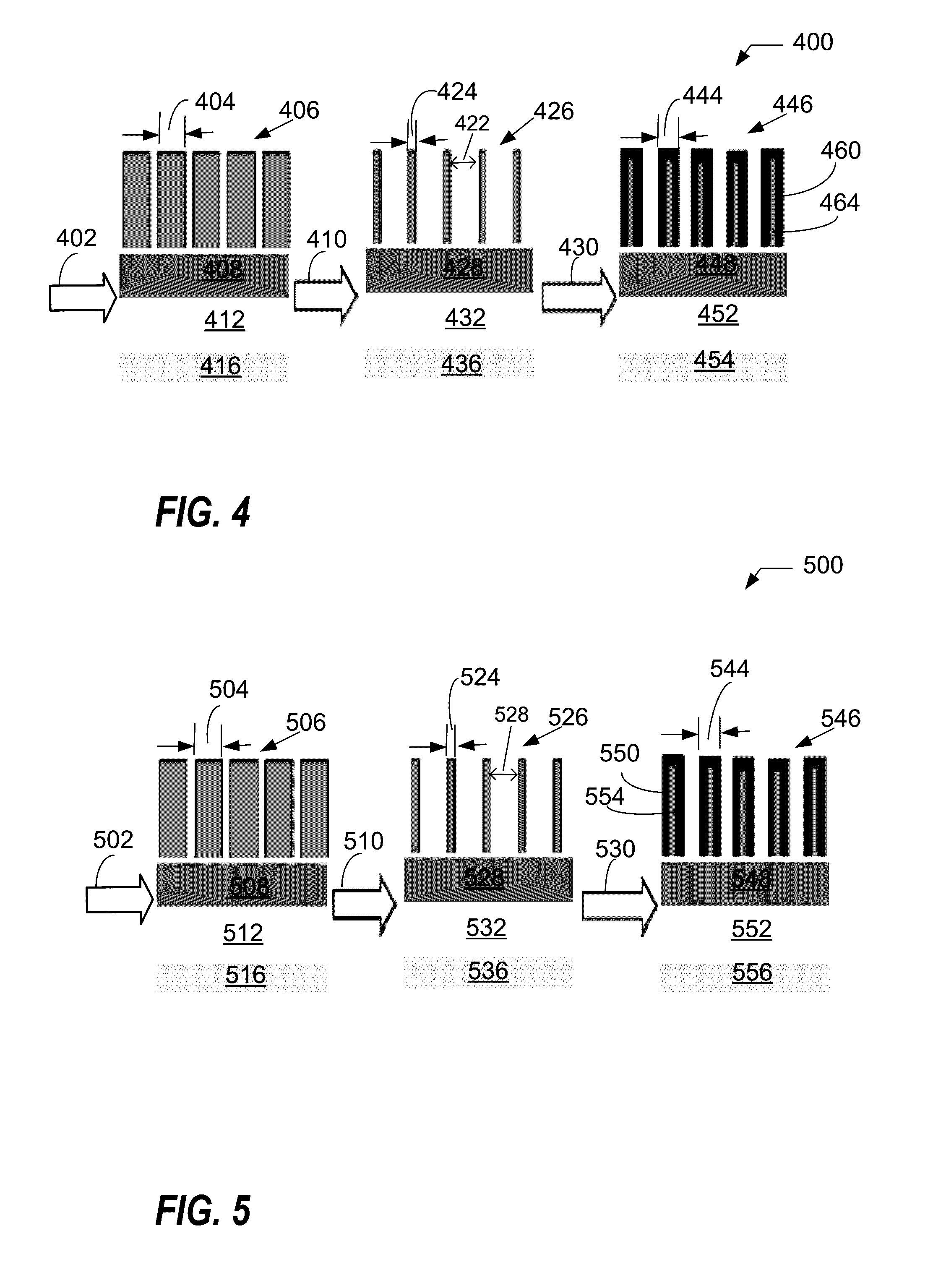
Provided is a method for patterning a substrate, comprising: forming a layer of radiation-sensitive material on a substrate; preparing a pattern in the layer of radiation-sensitive material using a lithographic process, the pattern being characterized by a critical dimension (CD) and a roughness; following the preparing the pattern, performing a CD shrink process to reduce the CD to a reduced CD; and performing a growth process to grow the reduced CD to a target CD. Roughness includes a line edge roughness (LER), a line width roughness (LWR), or both LER and LWR. Performing the CD shrink process comprises: coating the pattern with a hard mask, the coating generating a hard mask coated resist; baking the hard mask coated resist in a temperature range for a time period, the baking generating a baked coated resist; and developing the baked coated resist in deionized water.

Description

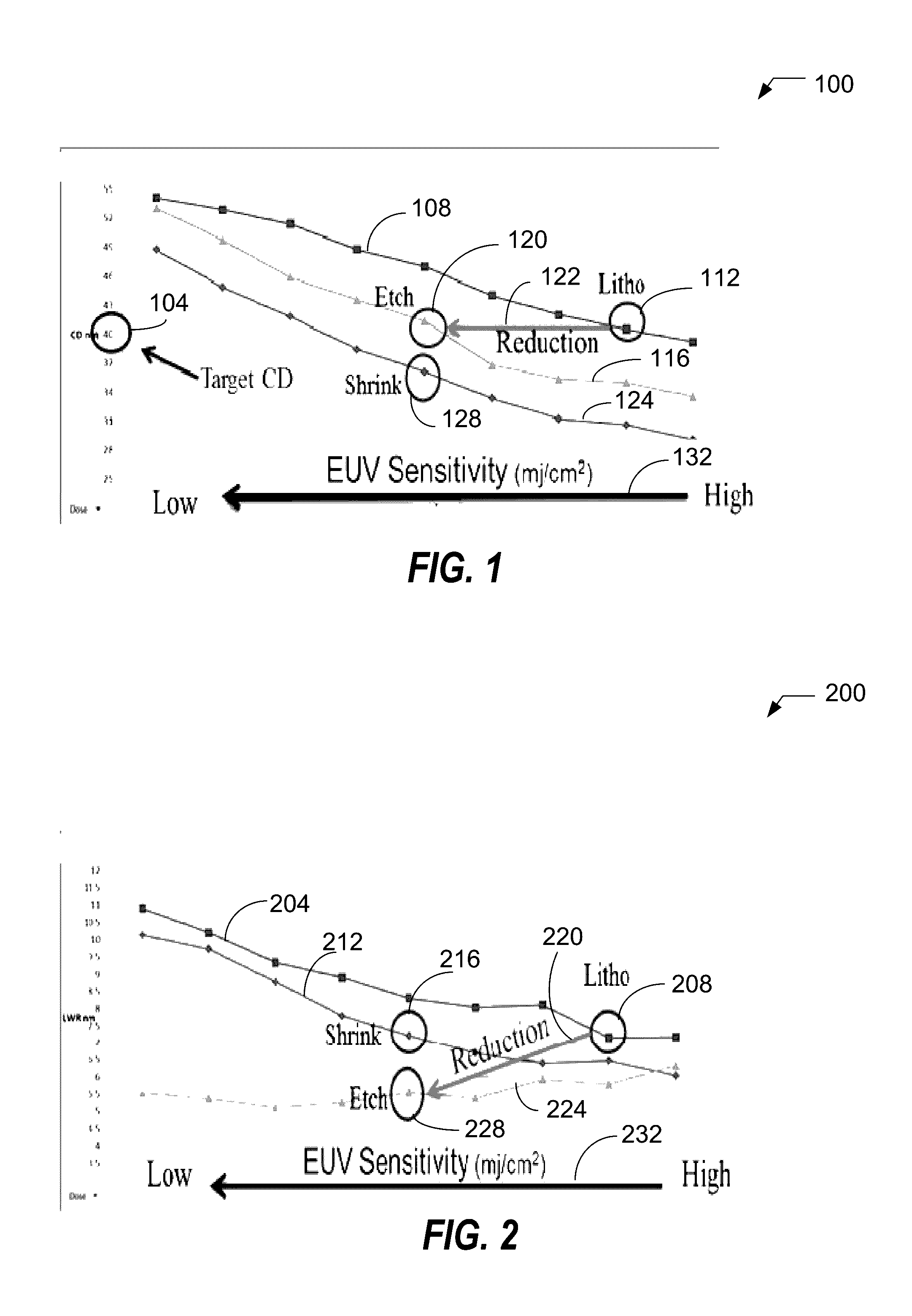
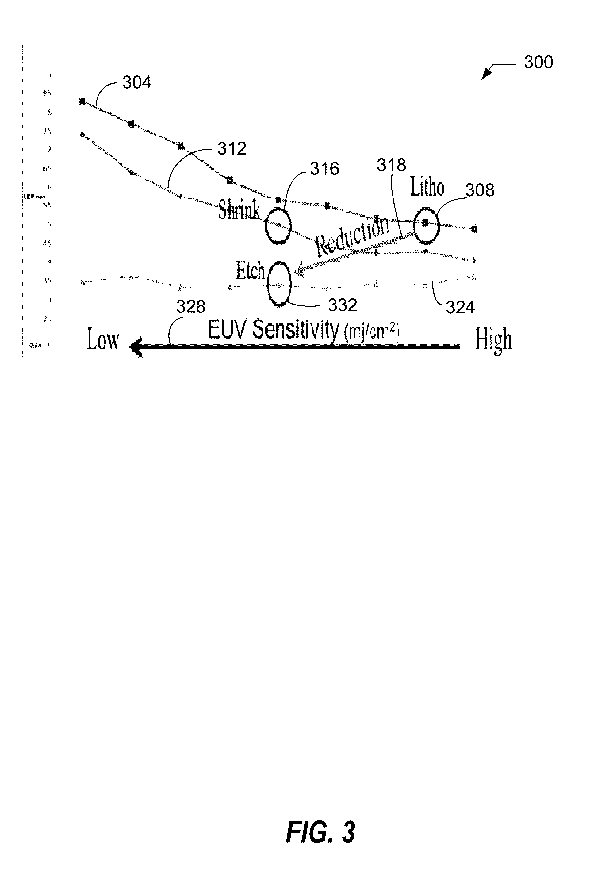
BACKGROUND OF THE INVENTION[0001]1. Field of Invention[0002]The invention relates to a method and systems for patterning a thin film on a substrate, and more particularly to a method and system for reducing resist sensitivity and improving line width roughness and line edge roughness or contact edge roughness.[0003]2. Description of Related Art[0004]In material processing methodologies, pattern etching comprises the application of a layer of radiation-sensitive material, such as photo-resist, to an upper surface of a substrate, the formation of a pattern in the layer of radiation-sensitive material using photo-lithography, and the transfer of the pattern formed in the layer of radiation-sensitive material to an underlying thin film on the substrate using an etching process. The patterning of the radiation-sensitive material generally involves exposure of the radiation-sensitive material to a pattern of electromagnetic (EM) radiation using, for example, a photo-lithography system, fo...

Claims


Application Information

Patent Timeline
Patent Type & Authority Applications(United States)
IPC IPC(8): G03F7/40G03F7/32G03F7/20
CPCG03F7/40G03F7/32G03F7/2004G03F7/70425G03F7/70625G03F1/22G03F1/34G03F1/80G03F7/168G03F7/70033G03F7/70958
Inventor HULI, LIORMOHANTY, NIHAR
Owner TOKYO ELECTRON LTD
Learn More