Front face and edge inspection

Active Publication Date: 2009-11-24
KLA TENCOR CORP
View PDF6 Cites 14 Cited by
  • Summary
  • Abstract
  • Description
  • Claims
  • Application Information

AI Technical Summary

Benefits of technology

[0018]In addition, the surface inspection tool and the edge inspection tool can be integrated inside an equipment front-end module (EFEM). As shown in FIG. 2, the edge inspection tool 204 and surface inspection tool 206 are integrated inside an EFEM 202, which reduces additional substrate delivery, load and align time. In embodiments such as those shown in FIGS. 1A-1B and FIG. 2, the edge inspection tool 202 may be configured to perform edge inspection of one or more substrates 203 while the surface inspection tool 206 performs surface inspection of a different substrate 201.
[0023]In 408, the bright field recipe may be automatically modified to allow scanning of the one or more of the additional substrates that are determined to be “at risk” based on results of the edge inspection. The bright field recipe may be modified to allow scanning of the “at risk” surface regions of the additional substrates. Edge defect patterns may be correlated to one or more processes to which the substrates are subjected prior to inspection. Modification of the bright field recipe may therefore depend on one or more process steps taking prior to the inspection process. For example, FIGS. 5A-5C illustrates three edge defect patterns for substrates that have undergone three different process steps. Knowledge of the edge defect pattern associated with the process step may be used to identify one or more at-risk regions on the surfaces of the substrates. It is noted that similar-looking edge defect patterns may lead to different assumptions about the at-risk region based on the nature of the process that the substrate has undergone. For example, FIG. 5A shows a pattern of edge defects 501 on a substrate 502 after a circular pattern process such as a Chemical Mechanical Planarization (CMP) process, which includes pressing a polishing “head” on the rotating substrate against a flexible pad. The rotationally symmetric nature of CMP combined with the observed pattern of defects 501 suggests one or more wedge-shaped at-risk regions 503. It is noted that this at-risk region is different from a potential reference area 504 that might otherwise be defined for the bright field recipe. The recipe may be modified to initially probe the at-risk region 503. This improves the chance that the modified recipe will locate defects more quickly than the unmodified recipe.
[0029]The surface and edge inspection systems as described in FIGS. 1A-1B and FIG. 2 and the method for inspecting substrates as described in FIG. 4 may allow for a decrease in sampling, e.g., to about 2-3 substrates per 20-substrate batch. Such a decrease in sampling may increase the substrate throughput and reduce the cost of ownership in a semiconductor manufacturing facility. Although the examples described above may relate to surface and edge inspection on semiconductor wafers, those of skill in the art will recognize that embodiments of the invention may be applied to surface and edge inspection of other substrates, such as reticles, flat panels, MEMS, optical lens and other manufacturing requiring the combination of front face and edge control.

Problems solved by technology

For instance, a large scratch, residual slurry or open blister on the bevel can flake or peel off, depositing particles on the front surface that cause the defects.
The current inspection tools and techniques are time consuming and require a large number of standard samples, which decreases the throughput in semiconductor manufacture.

Method used


Image

  • Front face and edge inspection
  • Front face and edge inspection
  • Front face and edge inspection

Examples


Embodiment Construction

[0012]Although the following detailed description contains many specific details for the purposes of illustration, anyone of ordinary skill in the art will appreciate that many variations and alterations to the following details are within the scope of the invention. Accordingly, the exemplary embodiments of the invention described below are set forth without any loss of generality to, and without imposing limitations upon, the claimed invention.

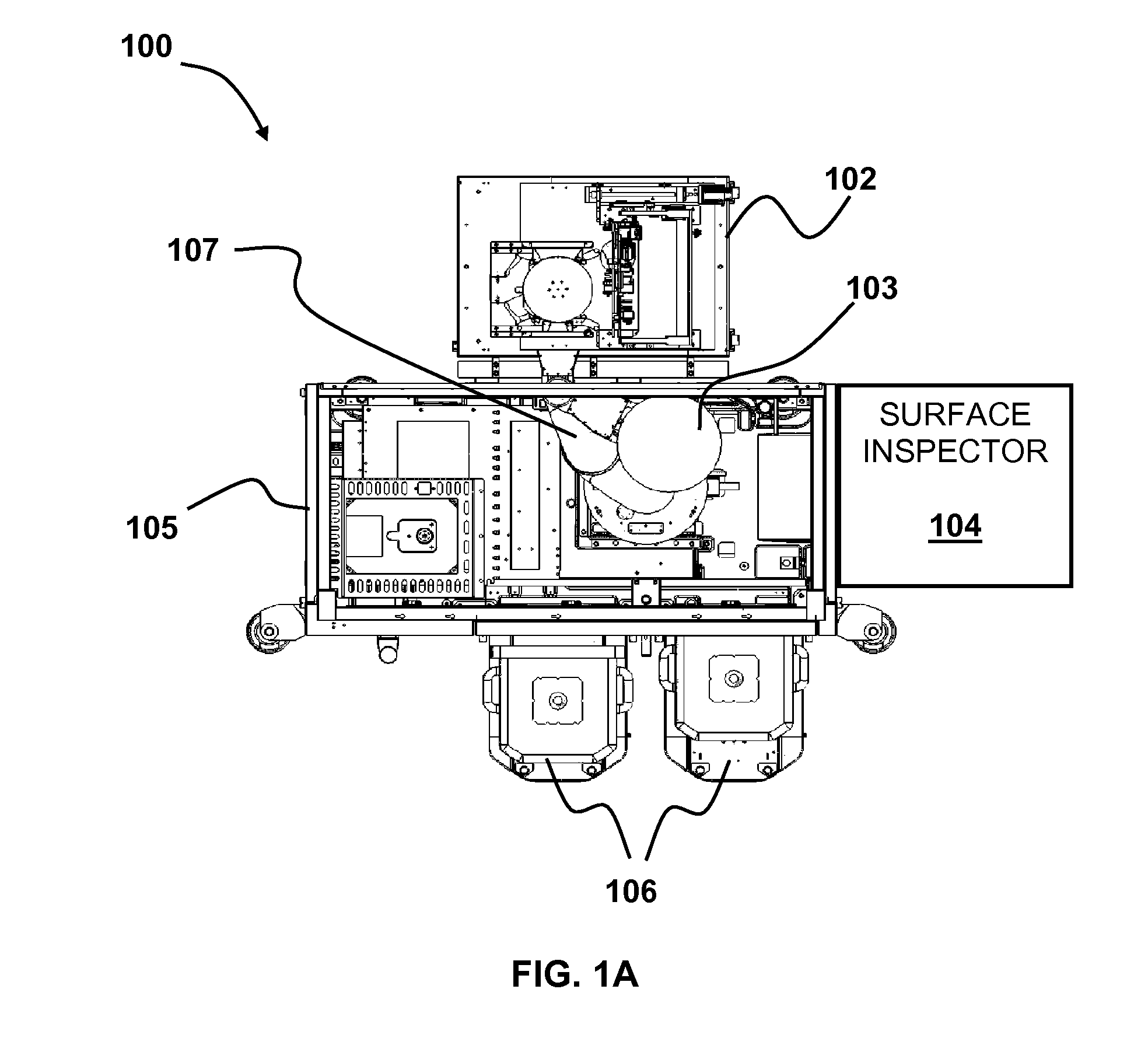
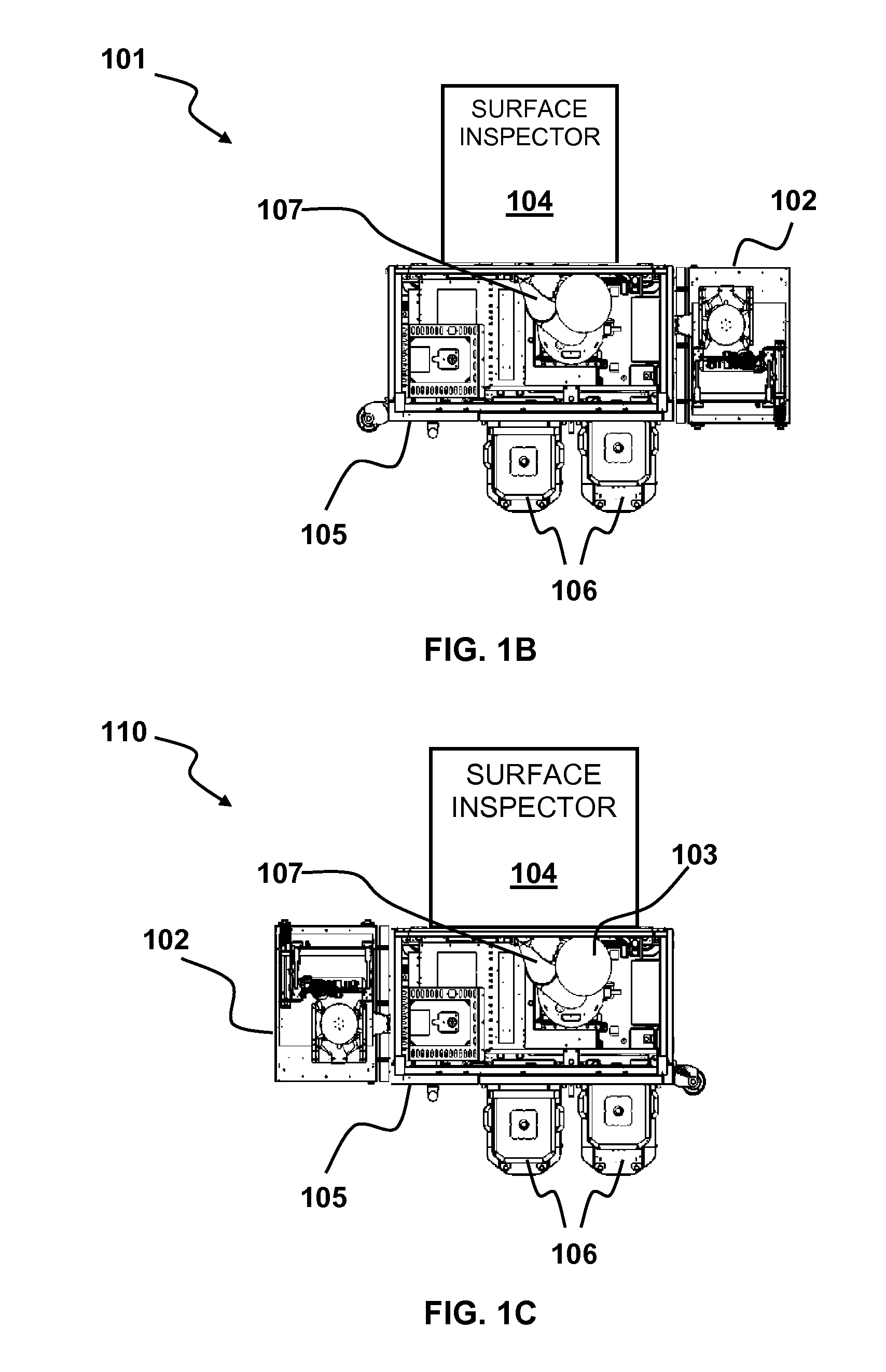
[0013]FIGS. 1A-1B are top views illustrating the surface and edge inspection systems according to an embodiment of the present invention. As shown in FIG. 1A, the surface and edge inspection system 100 may include a surface inspection tool 104 and an edge inspection tool 102. By way of example, the surface inspection tool 104 may be situated within an equipment front end module (EFEM) 105 that is adapted to receive one or more substrate pods 106. A transfer mechanism 107, such as a robot arm, may transfer substrates 103, e.g., semiconductor ...


PUM


Abstract

A surface and edge inspection system and the method for inspecting a substrate are disclosed. An edge inspection tool performs edge inspection of one or more substrates while a surface inspection tool performs surface inspection of a different substrate. A recipe for the surface inspection may be modified based on the results of the edge inspection.

Description

FIELD OF THE INVENTION[0001]This invention generally relates to surface inspection technique and more particularly to process combination of front face inspection and edge inspection.BACKGROUND OF THE INVENTION[0002]Semiconductor wafers may be inspected for defects such as, e.g., surface imperfections, particles, irregularities in the thickness of thin film coatings, and the like, which may hamper the performance of the semiconductor wafers. Some existing inspection systems direct a beam of radiation on the surface of the semiconductor wafers, then collect and analyze light reflected and / or scattered from the surface to quantify characteristics of the surface.[0003]Traditionally, the wafer edge has been of secondary concern to semiconductor manufactures, since it was considered a non-active area. However, there is a growing industry awareness that wafer edge conditions impact yields, directly and indirectly. For instance, a large scratch, residual slurry or open blister on the bevel...

Claims


Application Information

Patent Timeline
IPC IPC(8): G01N21/00
CPCG01N21/9501G01N21/9503G01N2021/9518G01N2021/8841
Inventor MUCKENHIRN, SYLVAIN
Owner KLA TENCOR CORP
Why Eureka
Try Eureka