
Photovoltaic device

a photovoltaic device and photovoltaic technology, applied in the field of photovoltaic devices, can solve the problems of large amount of energy, difficult synthesis and purification of organic hole transport materials, and limited success of dye solar cell devices in the market place, and achieves the effects of high conductivity, high hole mobility of inorganic hole transport materials, and easy production

Inactive Publication Date: 2016-07-28
DYESOL LTD
View PDF3 Cites 18 Cited by
  • Summary
  • Abstract
  • Description
  • Claims
  • Application Information

AI Technical Summary

Benefits of technology

The present invention utilizes the transparent character of inorganic hole transport materials to direct light towards the light absorber layer and provide effective conduction paths for photogenerated holes. This results in higher light-to-electricity conversion efficiency for solar devices. The invention also provides solar cells based on low-cost, inorganic materials of low toxicity, high stability, and easy to manufacture and process through low energy processes.

Problems solved by technology

Prior art photovoltaic technology is generally based on materials, which require large amounts of energy for their production, due to processing high temperature, often in excess of 1,000° C., due to very high demands in terms of purity and due the necessity of expensive, energy intensive and relatively slow high vacuum processing for some of the production steps.
While the latter technology is based on much lower temperature and much lower cost and faster processing steps, dye solar cell devices had only limited success in the market place, largely due to challenges with liquid organic electrolytes in terms of device sealing and high temperature stability.
Generally, such organic hole transport materials are difficult to synthesise and purify and therefore costly.
Organic hole transport materials tend to be sensitive to the higher temperatures experienced by solar devices (85° C. and higher on hot sunny days) and / or to UV irradiation, which can negatively impact a device's long term stability.
Such additives unfavourably increase materials and processing costs and can result in lower device stability.
TBP is toxic and a liquid with a boiling point below 200° C. Additionally, some of the additives, cobalt complexes in particular, lead to parasitic light absorption, which reduces the efficiency of a photovoltaic device.
Both effects result in lower device performance.

Method used


Image

  • Photovoltaic device
  • Photovoltaic device
  • Photovoltaic device

Examples


example 1

[0124]A first batch of Ni(OH)2 paste was made from NiCl2.6H2O and NaOH.Ni(OH)2 was washed with deionised water four times. Pluronic F-127 copolymer was used as a binder in combination with Ni(OH)2 in terpineol in a 4.6:5:13.4 weight ratio to prepare a paste. Thin Ni(OH)2 films were obtained by spin coating. MO was formed after heat treatment at 400° C. for 30 minutes, resulting in transparent films

example 2

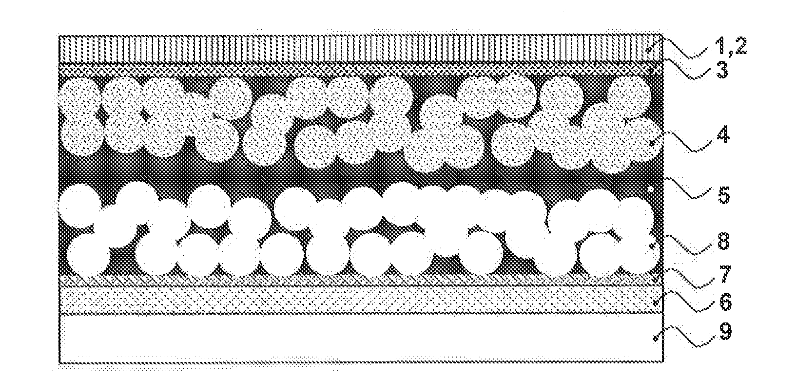
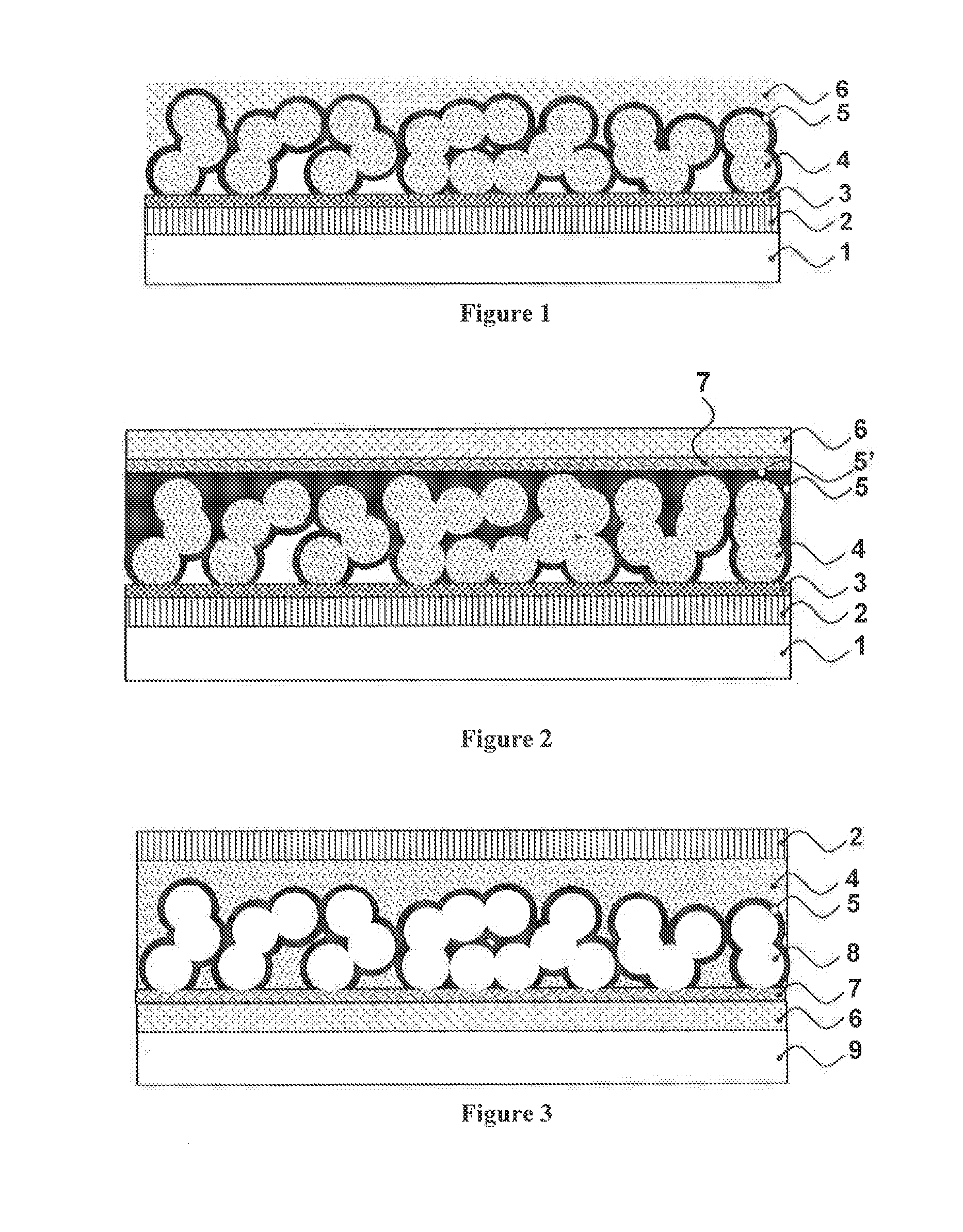
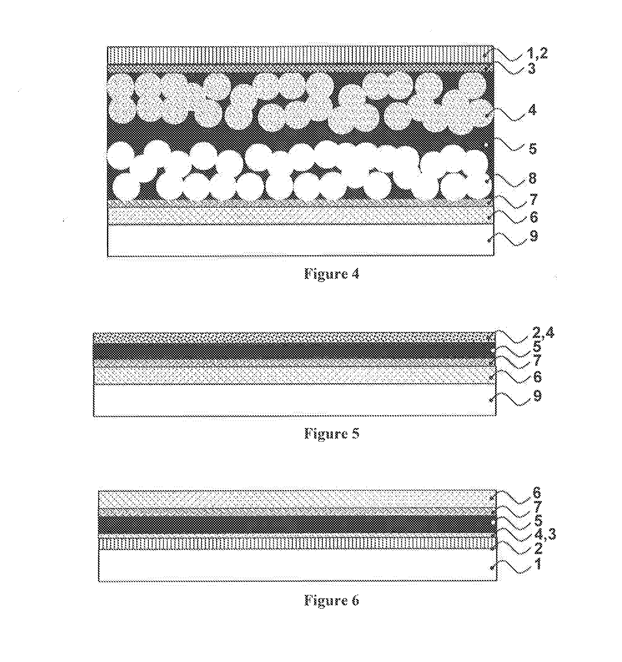
[0125]A thin TiO2 hole blocking layer was deposited on FTO / glass by ALD, followed by a thin coating of mesoporous Ties based on diluted Dyesol 18NRT TiO2 paste. CH3NH3PbI3 was then applied to the mesoporous TiO2 layer. Nano NiO, received from Sigma-Aldrich as a black powder. was dispersed into terpineol by mechanically stirring for 1 minute, followed by six passes in a three-roll mill. The ratio of NiO to terpineol was 1:3 wt:wt, NiO slurry was spin coated on top of the TiO2 / pervoskite layer using 2000 rpm for 20 seconds, followed by heating at 110° C., for 15 minutes. A thin layer of gold was deposited onto the NiO layer by vacuum evaporation, which resulted in a device according to configuration 2.

[0126]IV curves recorded immediately after assembly and after 5 days of storage, using a 0.285 cm2 mask during cell testing, are shown in FIG. 7 and key performance parameters are summarised in Table 1.

TABLE 1Cell IDNiOVoc (mV)initial653After 5 days671Jsc (mA / cm2)initial5.73After 5 days6...

example 3

[0127]A thin TiO2 hole blocking layer was deposited on FTO / glass by ALD, followed by a thin coating of mesoporous TiO2 based on diluted Dyesol 18NRT TiO2 paste. CH3NH3PbI3 was then applied to the mesoporous TiO2 layer. Nano NiO, received from Sigma-Aldrich as a black powder, was mixed in a 1:1 molar ratio with spiro-MeOTAD in chlorobenzene. spiro-MeOTAD concentration was 0.06M and 0.2M TBP and 0.03M LiTSFI were added to the mixture, however no cobalt dopant was employed. This slurry was spin coated on top of the TiO2 / pervoskite layer using 4000 rpm for 30 seconds in a dry air glove box. Subsequently, thin layer of gold was deposited onto the NiO / spiro-MeOTAD layer by vacuum evaporation, which resulted in a device according to configuration 3.

[0128]An IV curve, using a 0.159 cm2 mask during cell testing, is shown in FIG. 8 and key performance parameters are summarised in Table 2.

TABLE 2Cell IDNiO / spiro (1:1 mole ratio mixture)Voc (mV)788Jsc (mA / cm2)1.68Efficiency (%)0.75FF0.344


PUM


Abstract

Photovoltaic devices are described including: a region of perovskite material which is in electrical contact with a mesoporous region of hole transport material, wherein the hole transport material is at least partially comprised of an inorganic hole transport material.

Description

TECHNICAL FIELD[0001]This invention relates to photovoltaic devices and methods for preparing photovoltaic devices. This invention relates in particular to the internal architecture of solid state solar cells based on perovskite light absorbers and an inorganic hole transport material.BACKGROUND ART[0002]Electricity production from solar energy through photovoltaic devices holds great promise for a future with less reliance on fossil fuels. Prior art photovoltaic technology is generally based on materials, which require large amounts of energy for their production, due to processing high temperature, often in excess of 1,000° C., due to very high demands in terms of purity and due the necessity of expensive, energy intensive and relatively slow high vacuum processing for some of the production steps. More recently, dye solar cell technology has been developed based on liquid organic electrolytes. While the latter technology is based on much lower temperature and much lower cost and ...

Claims


Application Information

Patent Timeline
IPC IPC(8): H01L51/42H01L51/00
CPCH01L51/4226H01L2031/0344H01L51/0003H01L51/422Y02E10/549Y02P70/50Y02E10/542H10K71/12H10K71/50H10K30/151H10K85/50H10K30/50H01G9/2036H10K30/15
Inventor DESILVESTRO, HANSCAI, ZHIHONGJIANG, NANCY LAN
Owner DYESOL LTD
Learn More