
Use of silicon nitride as a substrate and a coating material for the rapid solidification of silicon

Inactive Publication Date: 2016-05-19
SACHS CHRISTOPH
View PDF2 Cites 0 Cited by
  • Summary
  • Abstract
  • Description
  • Claims
  • Application Information

AI Technical Summary

Benefits of technology

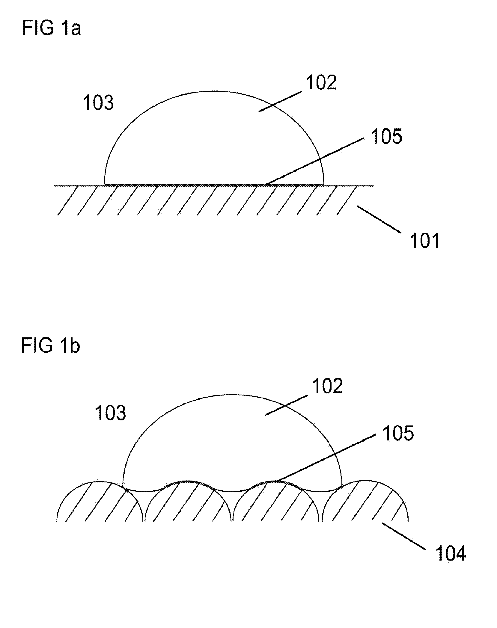
The invention describes the use of spherical silicon nitride particles as coating or substrate materials for kerfless wafer making technologies. These particles have low reactivity with molten silicon and low impurity content, making them suitable substrates for silicon wafer formation. Porous silicon nitride coatings or substrates made of spherical silicon nitride particles provide low nucleation rates, leading to the formation of silicon wafers with relatively large grain sizes. Using these materials can reduce the formation of unnecessary grain boundaries, improving the quality of silicon wafers.

Problems solved by technology

Bulk silicon nitride, however, is readily wetted by molten silicon.

Method used


Image

  • Use of silicon nitride as a substrate and a coating material for the rapid solidification of silicon
  • Use of silicon nitride as a substrate and a coating material for the rapid solidification of silicon
  • Use of silicon nitride as a substrate and a coating material for the rapid solidification of silicon

Examples


example 1

[0057]The effect of using silicon nitride powder to influence the grain size in a silicon wafer was demonstrated by forming grains in a monocrystalline silicon wafer as follows. The starting material used was an as-sawn monocrystalline silicon wafer having dimensions of 156 mm×156 mm and 200 μm thick, available from REC with headquarters in Norway. The silicon wafer was cleaved into 1″ wide and 4″ long pieces and coated with a thin layer of high-purity silicon nitride powder (SN E10 from UBE). The powder was in an aqueous solution, i.e., 15 wt % in DI water. The coating was applied by spraying the aqueous dispersion of the silicon nitride powder onto the silicon wafer using an airbrush. Before, during, and after the application of the coating, the silicon wafer was kept at a temperature above the boiling point of water, i.e., 120° C. so that the coating dried out quickly, i.e., within several seconds after application.

[0058]Referring to FIG. 6, the silicon wafer with the silicon nit...


PUM


Abstract

Silicon nitride particles are used as a coating or substrate material for kerfless wafer making technologies.

Description

CROSS REFERENCE TO RELATED APPLICATION[0001]This claims priority to and the benefit of provisional U.S. patent application Ser. No. 61 / 860,598 filed Jul. 31, 2013, the entirety of which is incorporated herein by reference.STATEMENT REGARDING FEDERALLY SPONSORED RESEARCH OR DEVELOPMENT[0002]This invention was made with Government support under Prime Contract No. DE-FG36-08GO18008, awarded by the Department of Energy. The Government has certain rights in this invention.TECHNICAL FIELD[0003]The invention generally relates to silicon nitride coatings for processing of silicon.BACKGROUND INFORMATION[0004]The majority of multicrystalline silicon wafers are produced by directionally solidifying silicon in a crucible and subsequently sawing the ingot into silicon wafers. In contrast, in kerfless silicon wafer making technologies, the silicon wafer or ribbon is directly formed from the silicon melt or by recrystallization of a silicon film. In several kerfless processes, molten silicon is in...

Claims


Application Information

Patent Timeline
IPC IPC(8): H01L31/18
CPCH01L31/182H01L31/186B22C3/00C30B11/00C30B11/002C30B11/003C30B11/02C30B19/00C30B19/067C30B19/12C30B29/06C30B35/002C30B28/06Y02E10/546Y02P70/50
Inventor SACHS, CHRISTOPH
Owner SACHS CHRISTOPH
Learn More