
Flexible Kesterite Photovoltaic Device on Ceramic Substrate

a photovoltaic device and flexible technology, applied in the field of flexible kesterite photovoltaic devices formed on ceramic substrates, can solve the problem of high cost of wide-scale production of cigs-based materials

Inactive Publication Date: 2016-05-05
IBM CORP +1
View PDF9 Cites 1 Cited by
  • Summary
  • Abstract
  • Description
  • Claims
  • Application Information

AI Technical Summary

Benefits of technology

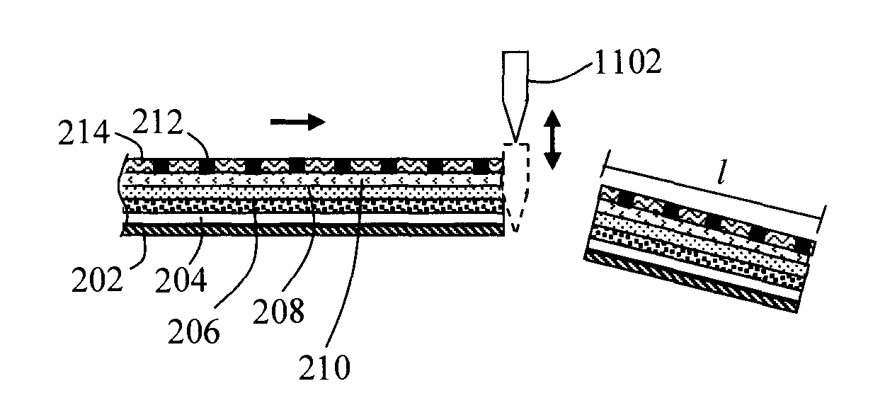
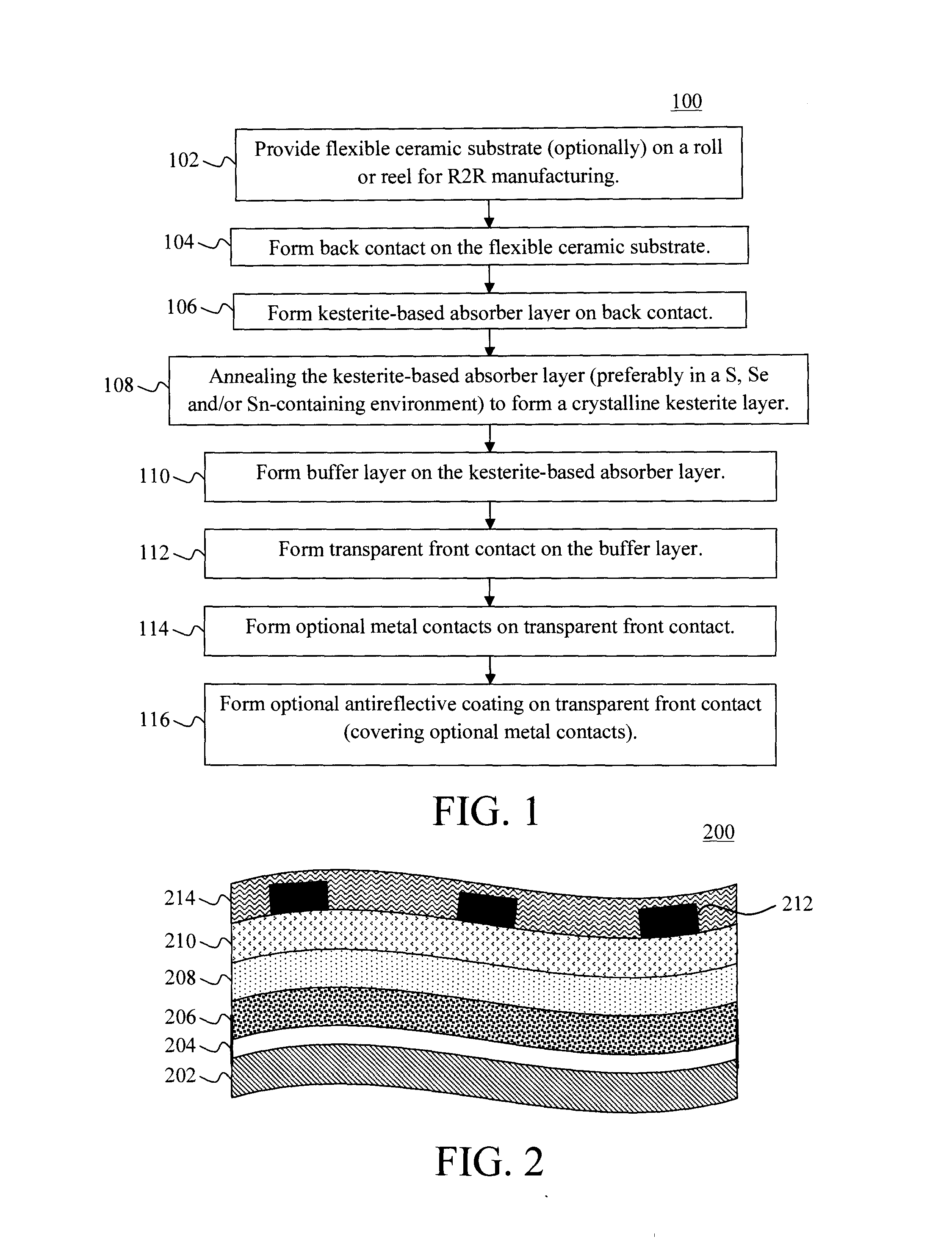
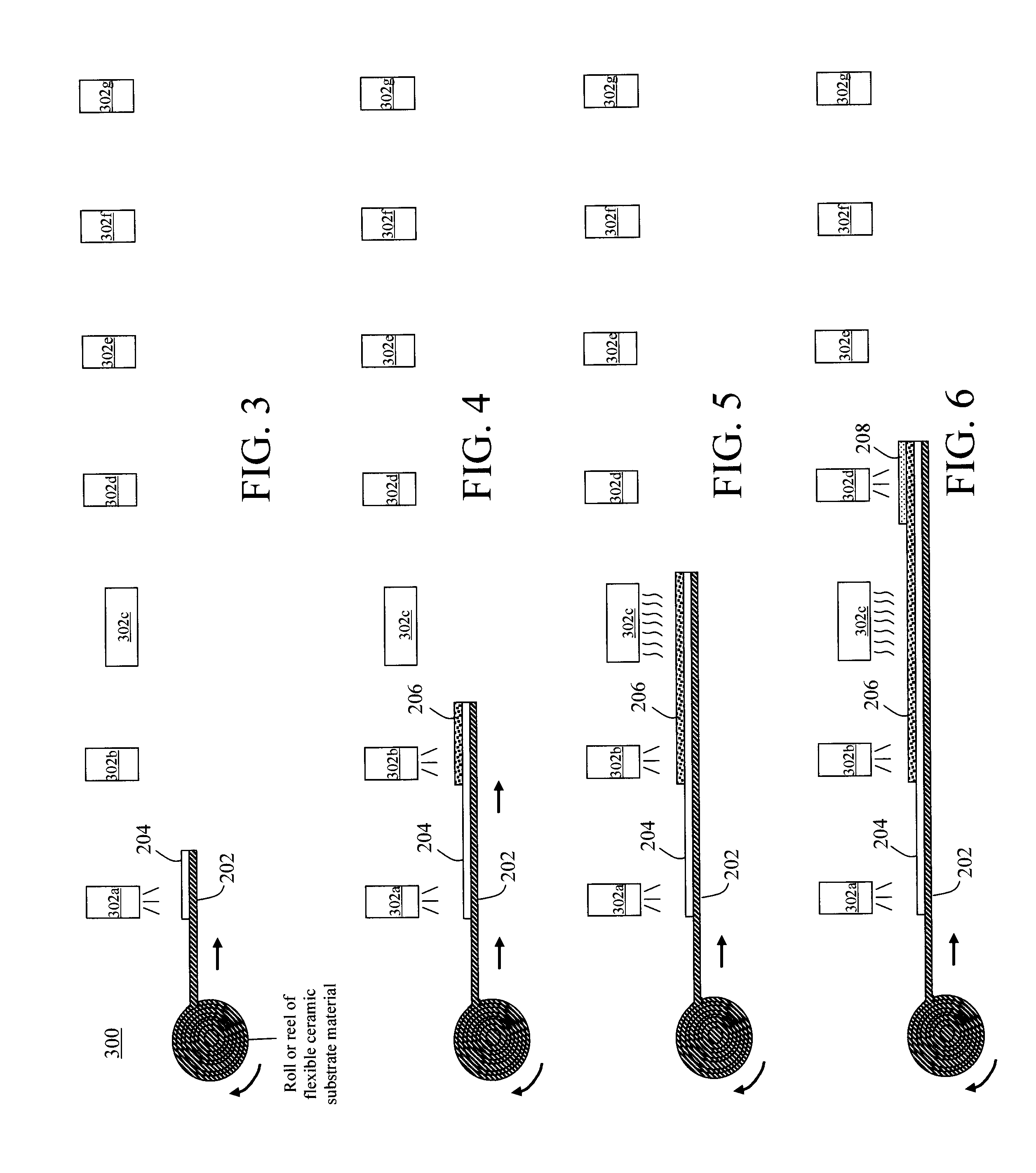
The present invention is about making photovoltaic devices using kesterite on flexible ceramic substrates. The invention provides a method for making a photovoltaic device by sequentially depositing layers of material onto a flexible ceramic substrate. There is also a method for making a kesterite-based photovoltaic device using a roll-to-roll approach. The invention provides a flexible photovoltaic device with improved efficiency and durability. The technical effects of this invention are improved performance and durability of photovoltaic devices using flexible ceramic substrates and kesterite absorber layers.

Problems solved by technology

Indium (a component of CIGS) is however a rare earth element, thus making the implementation of CIGS based materials expensive for wide scale production.

Method used


Image

  • Flexible Kesterite Photovoltaic Device on Ceramic Substrate
  • Flexible Kesterite Photovoltaic Device on Ceramic Substrate
  • Flexible Kesterite Photovoltaic Device on Ceramic Substrate

Examples


example 1

[0081]Zirconia discs (40-μm thick, 40 millimeter (mm) available from ENrG inc., Buffalo, N.Y.) were deposited with Mo layers by sputtering. Kesterite Cu2ZnSn(Se,S)4 layers were fabricated by spin-coating hydrazine solutions (method adapted from U.S. Patent Application Publication Number 2014 / 0096826). After a hot plate anneal in a sulfur-containing atmosphere at a temperature greater than about 540° C., solar cells were fabricated from the above-described Cu2ZnSn(Se,S)4 films by deposition of a 60 nanometer (nm) CdS buffer layer by chemical bath deposition, 100 nm insulating ZnO and 130 nm ITO (indium-doped zinc oxide) by sputtering, followed by nickel / aluminum metal contacts deposited by electron-beam evaporation.

[0082]A scanning electron micrograph (SEM) image of a solar cell produced according to Example 1 is shown in FIG. 13. This solar cell had a photovoltaic efficiency of 9.06% at 1.5 AM conditions, with open-circuit voltage (Voc)=0.483 Volts, short-circuit current density (Js...

example 2

[0083]flexible Zirconia substrates (available from ENrG inc., Buffalo, N.Y.) were deposited with Mo layers by sputtering. Kesterite Cu2ZnSn(Se,S)4 layers were fabricated by spin-coating hydrazine solutions (method adapted from U.S. Patent Application Publication Number 2014 / 0096826). After a hot plate anneal in a sulfur-containing atmosphere at a temperature greater than about 540° C., solar cells were fabricated from the above-described Cu2ZnSn(Se,S)4 films by deposition of a 60 nm CdS buffer layer by chemical bath deposition, 100 nm insulating ZnO and 130 nm ITO (indium-doped zinc oxide) by sputtering, followed by nickel / aluminum metal contacts deposited by electron-beam evaporation and finally a 110 nm antireflection coating of magnesium fluoride (MgF2).

[0084]A SEM image of a solar cell produced according to Example 2 is shown in FIG. 14. This solar cell had a photovoltaic efficiency of 11.5% at 1.5 AM conditions, with open-circuit voltage (Voc)=452 millivolts, short-circuit curr...


PUM


Abstract

Kesterite-based photovoltaic devices formed on flexible ceramic substrates are provided. In one aspect, a method of forming a photovoltaic device includes the steps of: forming a back contact on a flexible ceramic substrate; forming a kesterite absorber layer on a side of the back contact opposite the flexible ceramic substrate; annealing the kesterite absorber layer; forming a buffer layer on a side of the kesterite absorber layer opposite the back contact; and forming a transparent front contact on a side of the buffer layer opposite the kesterite absorber layer. A roll-to-roll-based method of forming a photovoltaic device and a photovoltaic device are also provided.

Description

FIELD OF THE INVENTION[0001]The present invention relates to photovoltaic devices and more particularly, to kesterite-based photovoltaic devices formed on flexible ceramic substrates, e.g., using roll-to-roll (R2R) manufacturing.BACKGROUND OF THE INVENTION[0002]Flexible ceramic substrates offer significant technological advantages over commonly used soda-lime glass substrates. For example, flexible ceramic substrates have extremely high temperature resistance (with a softening point twice that of glass), from about 40 to about 80 times lower mass and thermal budget (which translates to proportionally faster heating / cooling times and lower energy consumption) and roll-to-roll (R2R) manufacturing compatibility. These qualities can result in higher-efficiency photovoltaic devices (due to higher processing temperatures), as well as a lower-cost, less labor-intensive industrial process.[0003]The inertness and high temperature resistivity of ceramics is particularly important for material...

Claims


Application Information

Patent Timeline
IPC IPC(8): H01L31/032H01L31/0224H01L31/0392H01L31/0336H01L31/072H01L31/18H01L31/0216
CPCH01L31/0326H01L31/18H01L31/1884H01L31/1864H01L31/03926H01L31/02168H01L31/0336H01L31/072H01L31/022441Y02E10/50Y02P70/50
Inventor OLENICK, JOHN A.TODOROV, TEODOR K.
Owner IBM CORP
Learn More