
Patterning of electroless metals by selective deactivation of catalysts

a technology of electroless metals and catalysts, applied in the direction of superimposed coating process, resistive material coating, liquid/solution decomposition chemical coating, etc., can solve the problems of increasing the complexity and cost of fabrication, the method is expensive, and the method may not be used effectively for catalysts

Active Publication Date: 2016-04-21
AVERATEK
View PDF3 Cites 3 Cited by
  • Summary
  • Abstract
  • Description
  • Claims
  • Application Information

AI Technical Summary

Benefits of technology

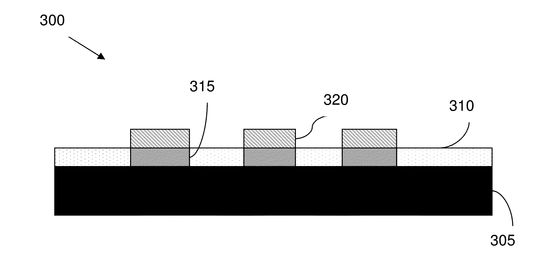
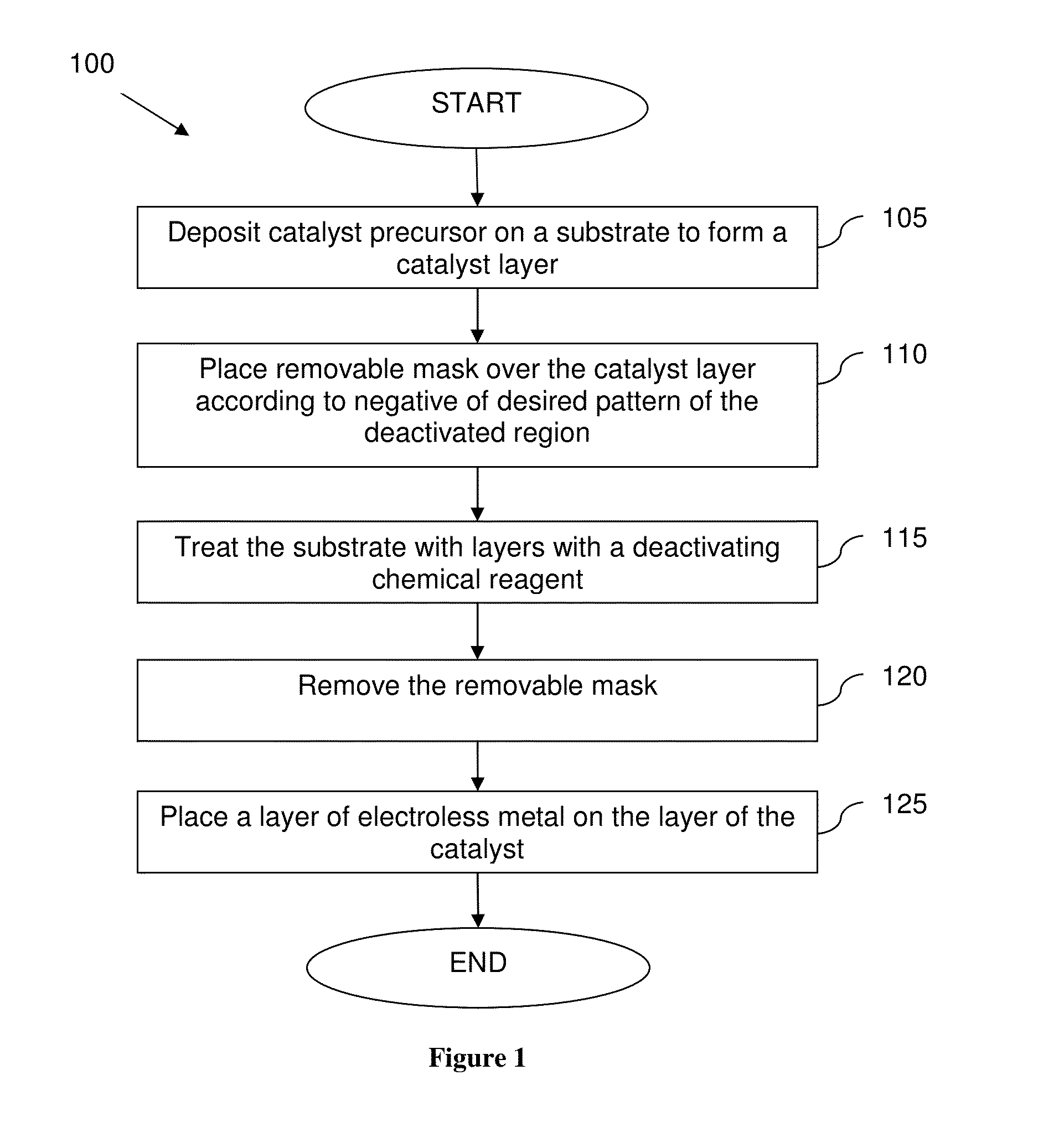
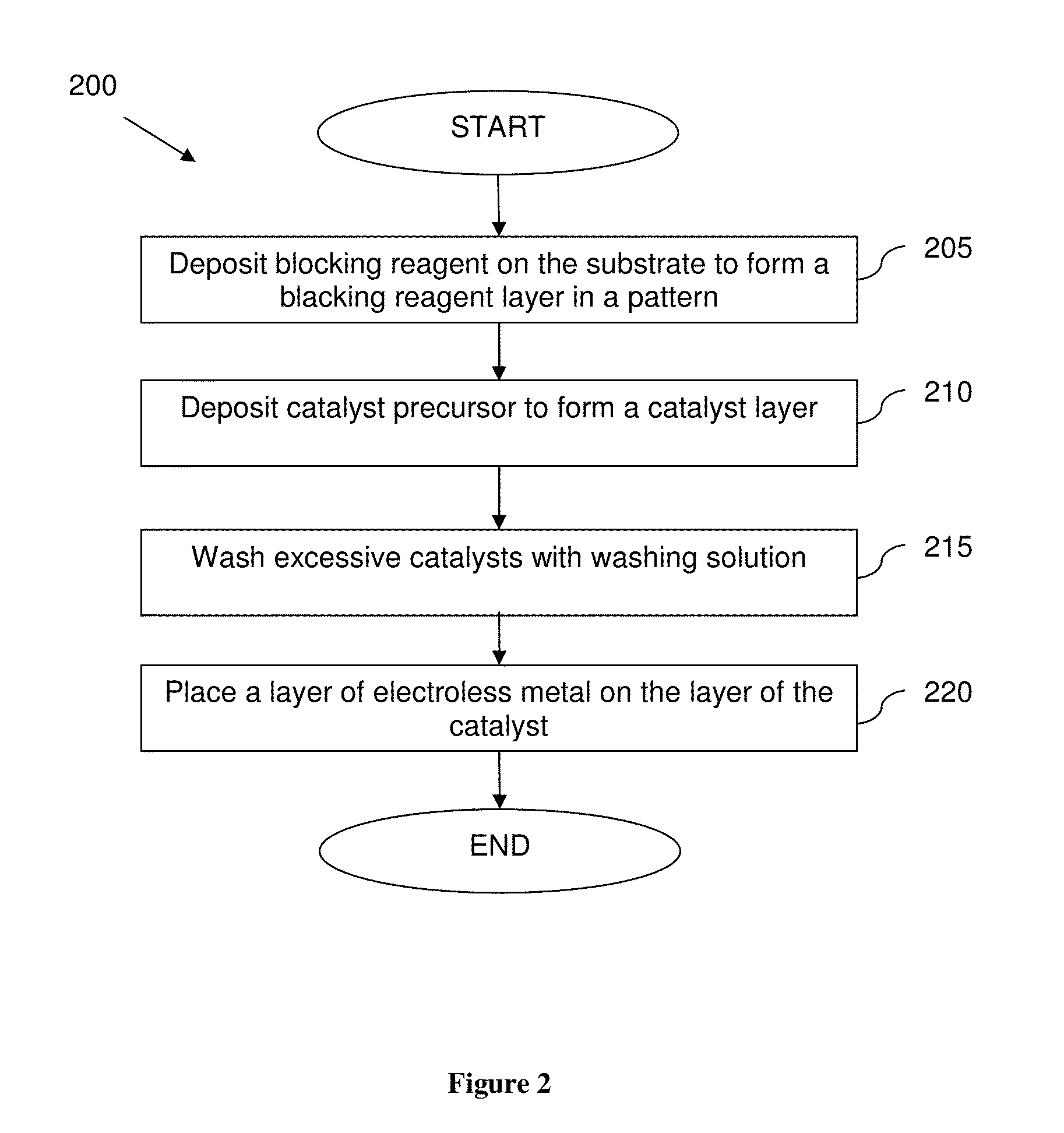
The patent text describes a method and device for patterning electroless metals. The method involves placing a catalyst layer on a substrate and then placing a mask layer with a circuit pattern over the catalyst layer to mask it. The exposed catalyst layer is then deactivated using a reagent. The mask layer is removed and the active catalyst layer is exposed to electroless metal composition to form a pattern of the metal on the substrate. The device includes a substrate coated with a first layer of blocking reagent in a pattern, followed by a second layer of catalyst, and a third layer of an electroless metal layer that is placed over the second layer of catalyst. The technical effect of this invention is to provide a precise and reliable method for patterning electroless metals, which can be useful in various applications such as electronics and sensors.

Problems solved by technology

Yet, such methods are expensive because it wastes a large portion of copper that is removed by etching steps, and is also time-consuming.
However, those methods may not be used effectively for catalysts that are not easily imageable to allow selective metallization in the form of an image.
In addition, many of those methods require multiple steps that increase the complexity and cost of fabrication.

Method used


Image

  • Patterning of electroless metals by selective deactivation of catalysts
  • Patterning of electroless metals by selective deactivation of catalysts
  • Patterning of electroless metals by selective deactivation of catalysts

Examples


examples

[0054]We have successfully used palladium (II) propionate and its complexes to deposit active palladium on substrates for electroless copper deposition. The field coated active palladium layer can be selectively deactivated by using sulfur compounds such as yellow ammonium sulfide or potassium polysulfide, etc. Selective patterning can be performed by masking the active layer of palladium deposited on a substrate by using masking agents that are benign to active palladium. The areas having unmasked palladium layer can be exposed to a solution of potassium polysulfide or yellow ammonium sulfide which deactivate the catalytic palladium. The benign masking agents can now be removed to expose active palladium followed by electroless metal deposition to form a pattern of the electrolessly deposited metal on the substrate.

[0055]Alternatively, metalized patterns for printed circuit boards can be created with methods include (1) using photolithographic imaging combined with subtractive etch...

example i

[0057]A substrate (e.g., a coupon) of 1 mil-thick polyimide was coated with a solution of amyl acetate containing 3000 ppm of palladium as palladium (II) propionate-cyclopentylamine complex as described in U.S. Pat. No. 8,110,254, which is incorporated in its entity by reference herein, and then heated to 300° C. for 10 minutes. A part of the substrate was dipped in an aqueous solution of potassium polysulfide (3000 ppm) for 1 minute. The substrate was then washed with deionized (DI) water and immersed in a commercial electroless copper solution M-22 supplied by MacDermid, Inc. The part of the substrate that was dipped in the solution of potassium polysulfide did not get deposition of electroless copper as shown in the FIG. 4.

example ii

[0058]A substrate (e.g., a coupon) of 1 mil-thick polyimide was coated with a solution of amyl acetate containing 3000 ppm of palladium as palladium (II) propionate-cyclopentylamine complex as described in U.S. Pat. No. 8,110,254, which is incorporated in its entity by reference herein, and then heated to 300° C. for 10 minutes. 5% Sb2S5 in Dimethyl sulfoxide (DMSO) heated to 160-180° C. and placed a palladium coated polyimide substrate (prepared as previously described) in the solution for 5-7 min. A similar substrate with palladium used as a control without a treatment with Sb2S5. The substrate without Sb2S5 could be plated with electroless copper while the Sb2S5 treated substrate could not be plated with electroless copper.


PUM

PropertyMeasurementUnit
temperatureaaaaaaaaaa
thicknessaaaaaaaaaa

Abstract

Methods and devices for patterning electroless metals on a substrate are presented. An active catalyst layer on the substrate can be covered with a patterned mask and treated with a deactivating chemical reagent, which deactivates the catalyst layer not covered by the mask. Once the patterned mask is removed, the electroless metal layer can be placed to have a patterned electroless metals. Alternatively, a substrate can be coated with a blocking reagent in a pattern first to inhibit formation of the catalyst layer before a catalyst layer can be placed over the blocking agent layer and then electroless metal layer is placed on the catalyst layer. The pattern of the blocking reagent acts as a negative pattern of the final conductive line pattern.

Description

[0001]This application claims priority to U.S. Provisional Patent Application No. 62 / 065,879 filed Oct. 20, 2014. Where a definition or use of a term in a reference that is incorporated by reference is inconsistent or contrary to the definition of that term provided herein, the definition of that term provided herein is deemed to be controlling.FIELD OF THE INVENTION[0002]The present invention relates to methods and systems for patterning electroless metals on a substrate. In particular, the present invention relates to methods and systems that utilize an inhibitor that deactivates catalysts in the selective area on the substrate.BACKGROUND[0003]The following description includes information that may be useful in understanding the present invention. It is not an admission that any of the information provided herein is prior art or relevant to the presently claimed invention, or that any publication specifically or implicitly referenced is prior art.[0004]Electroless metal deposition...

Claims


Application Information

Patent Timeline
Patent Type & Authority Applications(United States)
IPC IPC(8): H05K3/18H05K1/09
CPCH05K1/09H05K3/182H05K3/184C23C18/00C23C18/1608C23C18/161C23C18/1817C23C18/1841C23C18/1844C23C18/1865C23C18/1889C23C18/1893C23C18/2033C23C18/208C23C18/2086C23C18/30C23C18/32C23C18/38H05K2203/0565H05K2203/125
Inventor REDDY, MIHIRVINSON, MICHAEL RILEYSHARMA, SUNITY K.
Owner AVERATEK
Learn More