Wafer level integration of passive devices

a passive device and wafer technology, applied in the direction of basic electric elements, structural fixed capacitor combinations, inductances, etc., can solve the problems of high loss in such integrated circuit dies, complex process, cost addition,

Active Publication Date: 2016-03-31
APPLE INC
View PDF11 Cites 4 Cited by
  • Summary
  • Abstract
  • Description
  • Claims
  • Application Information

AI Technical Summary

Problems solved by technology

Further performance scaling may be limited without more efficient power delivery and power saving systems or techniques being developed.
Forming inductors and capacitors during CMOS processing, however, requires a complex process that can add cost, additional process time, require more masks, and / or more equipment.
Because of the complexity involved in forming the inductors and capacitors on the integrated circuit die during the CMOS process, the yield loss in such integrated circuit die may be high, which leads to additional manufacturing time and cost.
Additionally, because the inductors and capacitors are formed during the CMOS process, the specifications of the inductors and capacitors are limited by the CMOS process parameters.
Providing the inductors and capacitors on-package, however, may require large amounts of real estate space for the components, involve difficult physical routing, and be electrically inefficient with electrical losses.

Method used


Image

  • Wafer level integration of passive devices
  • Wafer level integration of passive devices
  • Wafer level integration of passive devices

Examples


Embodiment Construction

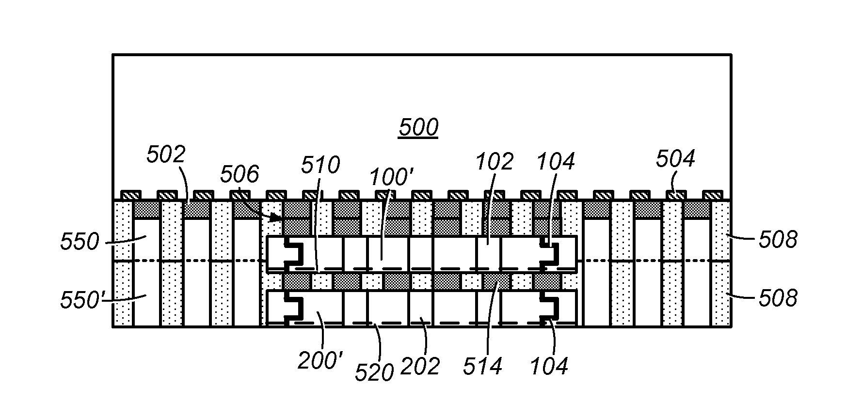
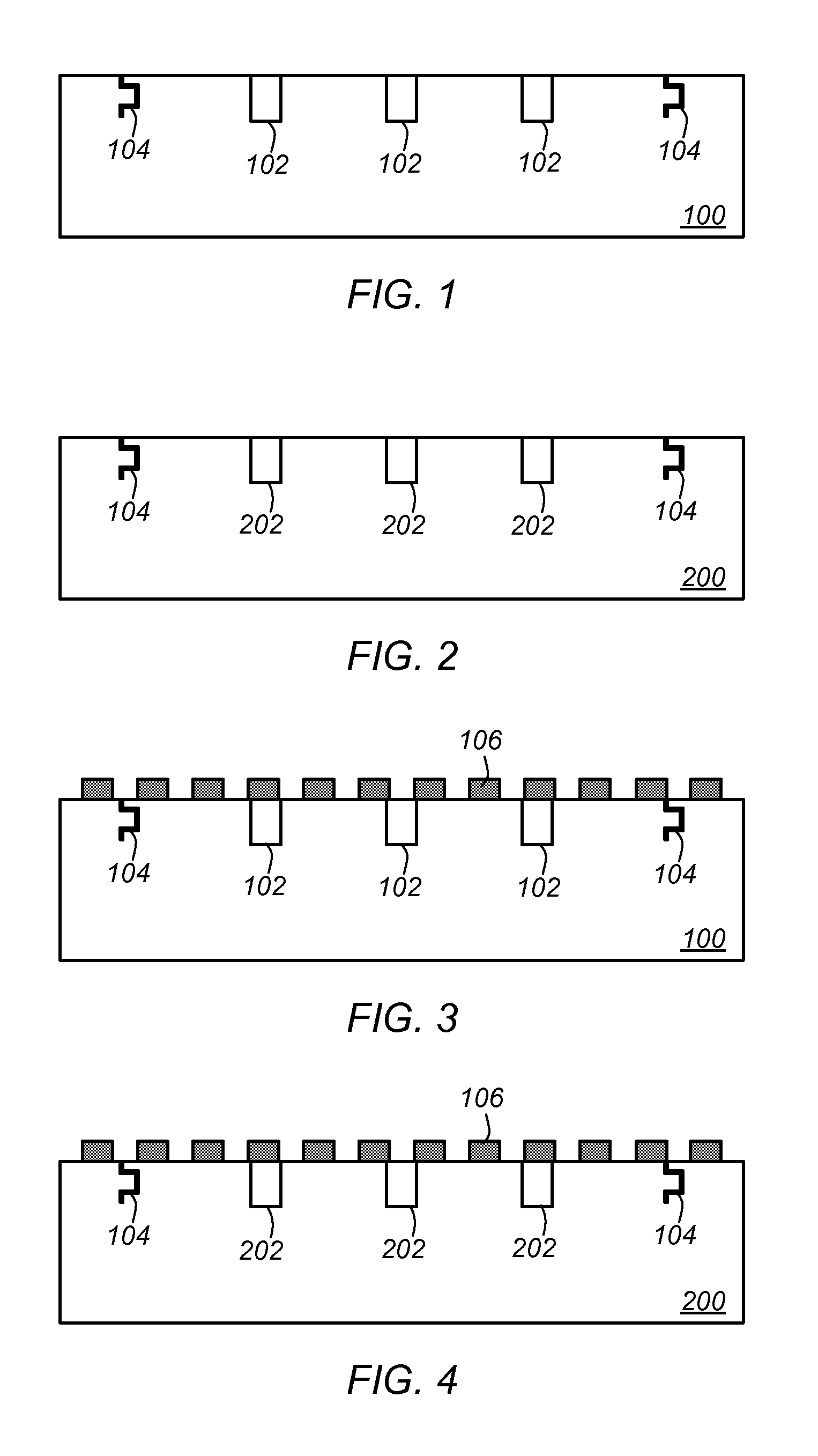
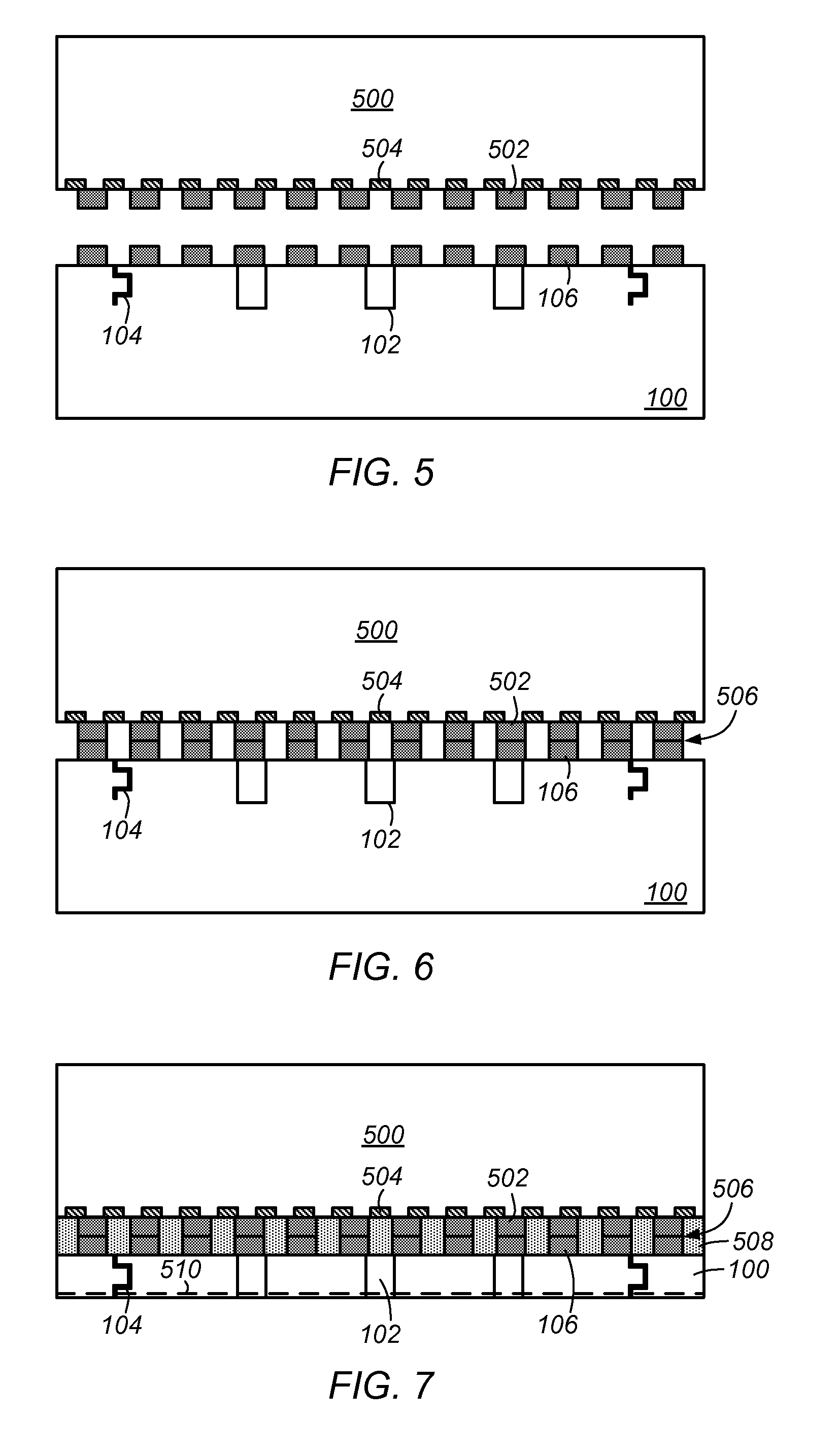
[0031]FIG. 1 depicts a cross-sectional side-view representation of an embodiment of a semiconductor substrate with passive devices and interconnects formed on the substrate. Substrate 100 may be a semiconductor substrate such as, but not limited to, a silicon substrate or a silicon wafer. In certain embodiments, passive devices 102 are formed on or in substrate 100. In certain embodiments, passive devices 102 are inductors. For example, passive devices 102 may be thin film inductors.

[0032]In certain embodiments, interconnects 104 are formed in substrate 100. Interconnects 104 may be partial vias or other three-dimensional interconnects formed in substrate 100 that are filled with conductive material (e.g., a metal such as copper). For example, interconnects 104 may be copper pillars or copper / solder pillars in substrate 100. Passive devices 102 and / or interconnects 104 may have a selected maximum depth in substrate 100. The selected maximum depth may allow portions of passive device...


PUM


Abstract

A semiconductor device is described that includes an integrated circuit coupled to a first semiconductor substrate with a first set of passive devices (e.g., inductors) on the first substrate. A second semiconductor substrate with a second set of passive devices (e.g., capacitors) may be coupled to the first substrate. Interconnects in the substrates may allow interconnection between the substrates and the integrated circuit. The passive devices may be used to provide voltage regulation for the integrated circuit. The substrates and integrated circuit may be coupled using metallization.

Description

PRIORITY CLAIM[0001]This patent claims priority to U.S. Provisional Patent Application No. 62 / 056,711 to Zhai, entitled “WAFER LEVEL INTEGRATION OF PASSIVE DEVICES”, filed Sep. 29, 2014, which is incorporated by reference in its entirety.BACKGROUND[0002]1. Technical Field[0003]Embodiments described herein relate to systems and methods for implementing power supply regulation in semiconductor devices. More particularly, the embodiments described herein relate to semiconductor devices with integrated passive devices for voltage regulation.[0004]2. Description of Related Art[0005]Power delivery along with power saving are increasingly factoring into integrated circuit device performance scaling for system on a chip (SoC) devices, central processing units (CPUs), and graphical processing units (GPUs). Delivering power more quickly to a device can increase the speed and power of the device while saving power by reducing losses during power transitions (e.g., powering on / off of the device...

Claims


Application Information

Patent Timeline
Patent Type & Authority Applications(United States)
IPC IPC(8): H01L25/065H01L21/56H01L21/683H01L21/768H01L21/78H01L23/00H01L23/31H01L23/528H01L25/00H01L49/02
CPCH01L25/0657H01L2225/06548H01L28/10H01L28/40H01L23/528H01L21/78H01L21/6835H01L21/768H01L24/09H01L24/89H01L21/56H01L23/3107H01L2221/68327H01L2224/0812H01L2224/80001H01L2225/06555H01L25/50H01L23/3114H01L24/14H01L24/94H01L24/97H01L25/16H01G4/40H01L2224/13147H01L2224/131H01L2224/73204H01L2224/32265H01L2224/32013H01L2224/1403H01L2224/16238H01L2224/16235H01L2224/16268H01L2224/2919H01L2224/81005H01L2224/81193H01L2924/14H01L2924/1432H01L2224/92125H01L2224/94H01L2224/97H01L2924/19042H01L2924/19041H01L2924/19104H01L2924/37001H01L2924/014H01L2224/81H01L2224/83H01L23/49822H01L23/50H01L24/16H01L2224/16227H01L2224/14181H01L2224/83104H01L2224/9202H01L24/13H01L24/29H01L2224/32225H01L24/32H01L2224/81447H01L2224/05599H01L2924/00014H01L2224/16225H01L2924/00H01L2924/0665H01L24/00
Inventor ZHAI, JUN
Owner APPLE INC
Why Eureka
Try Eureka