
Read Assist Techniques in a Memory Device

a memory device and assist technology, applied in the field of memory devices, can solve the problems of lowering stability, low operating voltage, process variation or low operating voltage, and known techniques are susceptible to process and temperature variation, and achieves simple provisioning configuration, reduced asserted voltage, and easy configuration

Active Publication Date: 2015-12-24
ARM LTD
View PDF14 Cites 11 Cited by
  • Summary
  • Abstract
  • Description
  • Claims
  • Application Information

AI Technical Summary

Benefits of technology

The present invention provides a memory device with a read assist circuitry that selectively reduces the voltage on a selected wordline when a read access is required. This reduction is achieved by selectively coupling the selected wordline to another wordline using a transistor connection. The transistor connection recognizes that the other wordlines are inactive and can thus be used for reducing the voltage on the selected wordline. The transistor connection is made using a selectable connection between two outermost wordlines, which allows for a more dense layout configuration. The read assist circuitry can also be implemented using a voltage divider and a selectable connection between the selected wordline and a reference voltage, which further protects against electrostatic discharge risks. The control over the selected connection can be generated entirely internally to the memory device.

Problems solved by technology

Such lowered stability can for example result from process variation or low operating voltages.
Various techniques are known for achieving this lowered voltage on the word line, such as charge injection / extraction solutions, which seek to vary the word line voltage by selectively connecting a capacitive element to it, yet these known techniques are susceptible to process and temperature variation.

Method used


Image

  • Read Assist Techniques in a Memory Device
  • Read Assist Techniques in a Memory Device
  • Read Assist Techniques in a Memory Device

Examples


Embodiment Construction

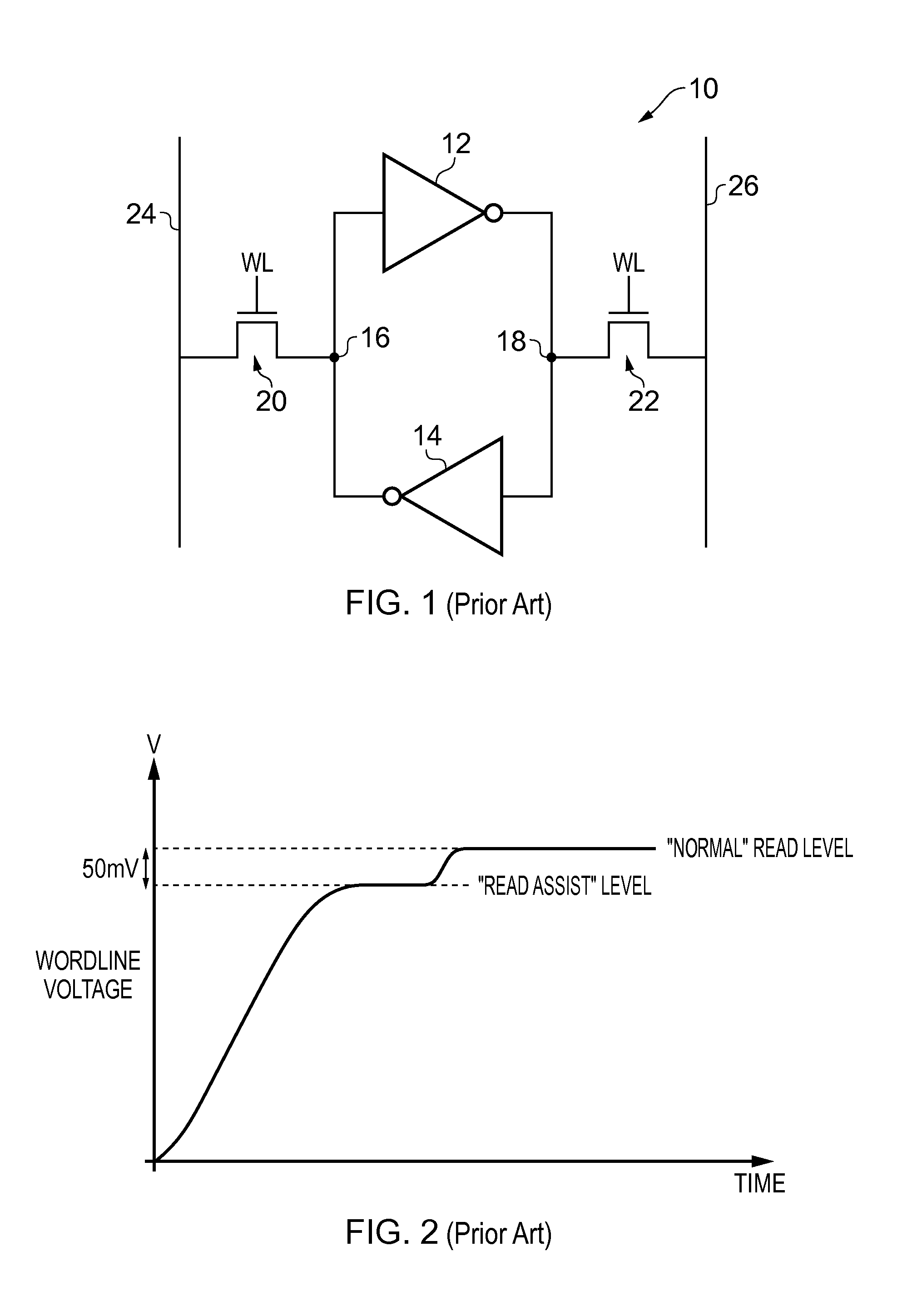
[0039]FIG. 1 schematically illustrates a known memory cell 10 which essentially consists of a pair of cross-coupled inverters 12 and 14. The configuration of these inverters 12 and 14 is such that the bit cell 10 can stably hold a pair of complementary values at the nodes 16 and 18. A pair of access transistors 20, 22 couples the nodes 16, 18 to the bit lines 24, 26 to enable the pair of values held at the nodes 16, 18 to be written and read out. In order to improve the read stability of the bit cell 10, when a read operation is carried out the word line voltage is asserted as is shown in FIG. 2, wherein the wordline voltage is temporarily held back from reaching the “normal” read level at a “read assist” level which is approximately 50 mV below it. One of ordinary skill in the art will be familiar with the manner in which this reduction in the word line read voltage helps to prevent the content of the bit cell 10 from being disturbed by the read process and further description ther...


PUM


Abstract

A memory device is provided which comprises an array of bitcells and a plurality of wordlines. Each bitcell of the array of bitcells is selectively coupled to a wordline of the plurality of wordlines and access to a selected bitcell of the array of bitcells requires an asserted voltage on a selected wordline with which the selected bitcell is associated. Read assist circuitry is provided, which is configured, when read access to the selected bitcell is carried out, to implement a reduction in the asserted voltage on the selected wordline, and wherein the read assist circuitry is configured to implement the reduction in the asserted voltage by selective connection of the selected wordline to a further wordline of the plurality of wordlines.

Description

FIELD OF THE INVENTION[0001]The present invention relates to a memory device. More particularly, it relates to read assist techniques when operating the memory device.BACKGROUND OF THE INVENTION[0002]As contemporary memories have progressed towards ever smaller process scales and lower operating voltages, it is known that it may be necessary to take steps to ensure that read stability is maintained. This relates to the fact that the configuration of a contemporary memory may be at a level where the access disturbance margin (ADM) or static noise margin (SNM) may be such that the action of reading a data bit held by a bit cell of the memory may cause the value of that data bit to change. Such lowered stability can for example result from process variation or low operating voltages.[0003]One known technique for addressing this problem is to lower the voltage applied to the relevant word line for at least part of the read process. By applying a lower voltage to the bit cell access port...

Claims


Application Information

Patent Timeline
Patent Type & Authority Applications(United States)
IPC IPC(8): G11C7/00
CPCG11C7/00G11C11/418G11C8/08G11C11/413G11C5/14G11C8/10
Inventor VAN WINKELHOFF, NICOLAASBRUN, MIKAELBLANC, FABRICE
Owner ARM LTD
Learn More