
Three-terminal spin transistor magnetic random access memory and the method to make the same

a technology of magnetic random access memory and three-terminal spin transistor, which is applied in the direction of magnetic field-controlled resistors, semiconductor devices, galvano-magnetic material selection, etc., can solve the problems of information readout errors increasing, value changes, and element unrecordable, so as to reduce the switching energy barrier of the recording layer, the effect of easy switching or revers

Inactive Publication Date: 2015-12-17
T3MEMORY
View PDF5 Cites 12 Cited by
  • Summary
  • Abstract
  • Description
  • Claims
  • Application Information

AI Technical Summary

Benefits of technology

This patent describes a memory cell that uses a special circuit design to change the magnetization of a recording layer using a low spin transfer current. The circuitry includes a bit line and a digital line that work together to decrease the energy barrier needed to switch the magnetization. This allows for easier and faster switching of the recording layer. The technical effect of this invention is to improve the performance and speed of magnetoresistive memory cells.

Problems solved by technology

More, even when the tunnel barrier does not immediately break down, if recording operations are repeated, the element may still become nonfunctional such that the resistance value changes (decreases) and information readout errors increase, making the element un-recordable.
Furthermore, recording is not performed unless a sufficient voltage or sufficient spin current is applied.
Accordingly, problems with insufficient recording arise before possible tunnel barrier breaks down.
However, patterning of small MTJ element leads to increasing variability in MTJ resistance and sustaining relatively high switching current or recording voltage variation in a STT-MRAM.
Any fluctuation in the electrical characteristics of individual MTJs at advanced technology nodes could cause what was intended as a read-current, to have the effect of a write-current, thus unintentionally reversing the direction of magnetization of the recording layer in MTJ.
Above issues or problems are all associated with the traditional two-terminal MRAM configuration.

Method used


Image

  • Three-terminal spin transistor magnetic random access memory and the method to make the same
  • Three-terminal spin transistor magnetic random access memory and the method to make the same
  • Three-terminal spin transistor magnetic random access memory and the method to make the same

Examples


Embodiment Construction

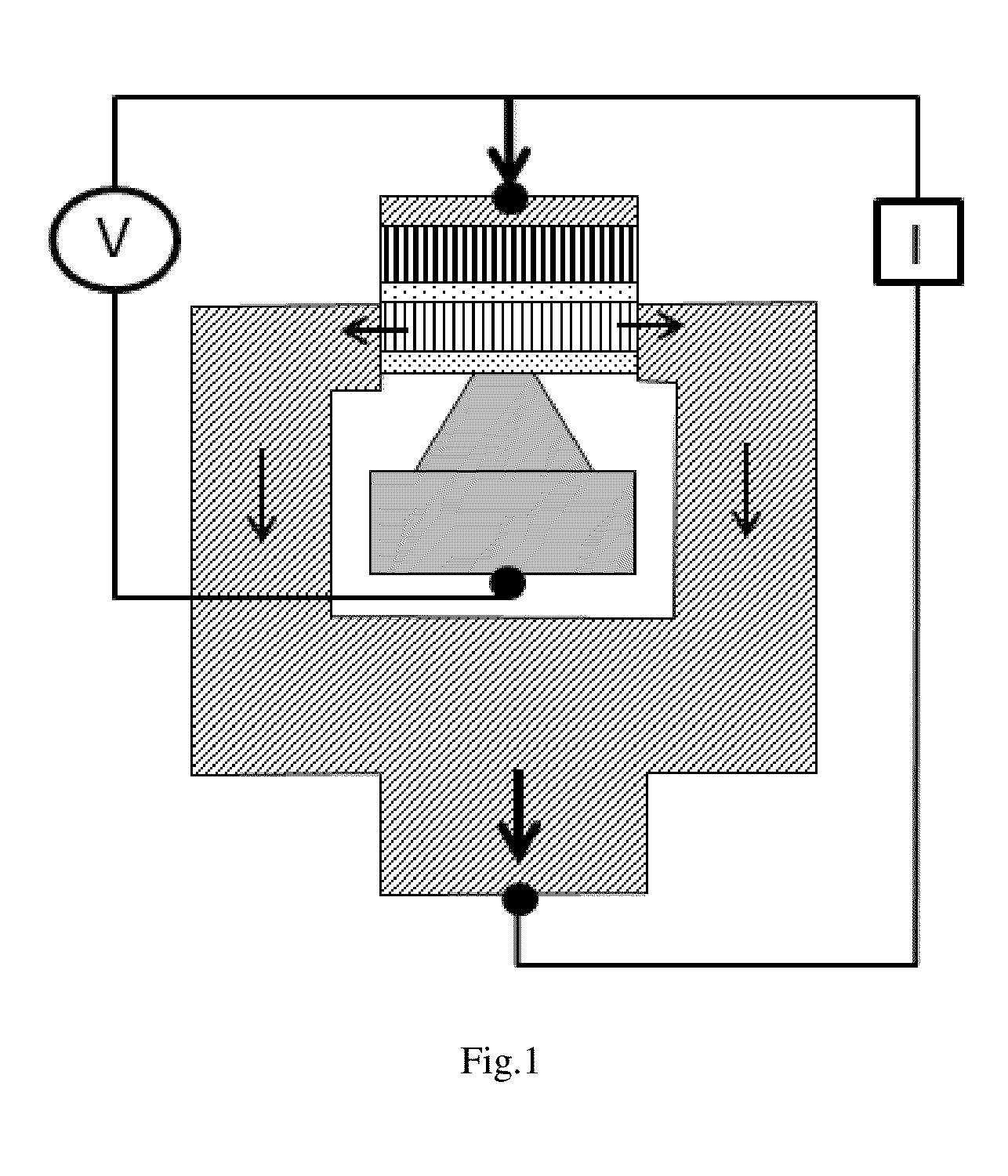
[0036]The three-terminal spin transistor magnetic random access memory (FIG. 1) contains a digital line at the bottom, a bit line on the top, and a magnetic memory cell in the middle. The middle memory cell has a bottom insulating layer (ILD), a magnetic memory layer, a dielectric MgO tunneling layer, a top reference layer, a cap layer and hard mask. The top reference layer has perpendicular magnetization to the plane, and the polarization of the middle memory layer can be either perpendicular to the plane or in the plane depending on the voltage applied between the top bit line and bottom digital line. Both read and write current flow through the top reference layer, middle memory film stack and VIA to / from the underneath CMOS control circuit (not shown). The digital line has a small contact area with the insulating layer below the memory cell which helps to reduce writing current when a voltage pulse is applied.

[0037]The fabrication process flow is shown in FIG. 2 which starts fro...


PUM


Abstract

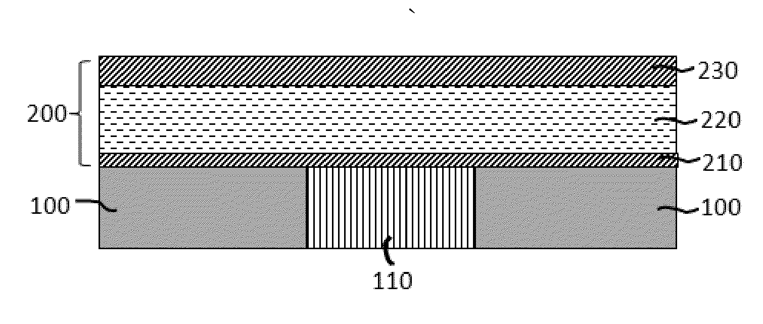
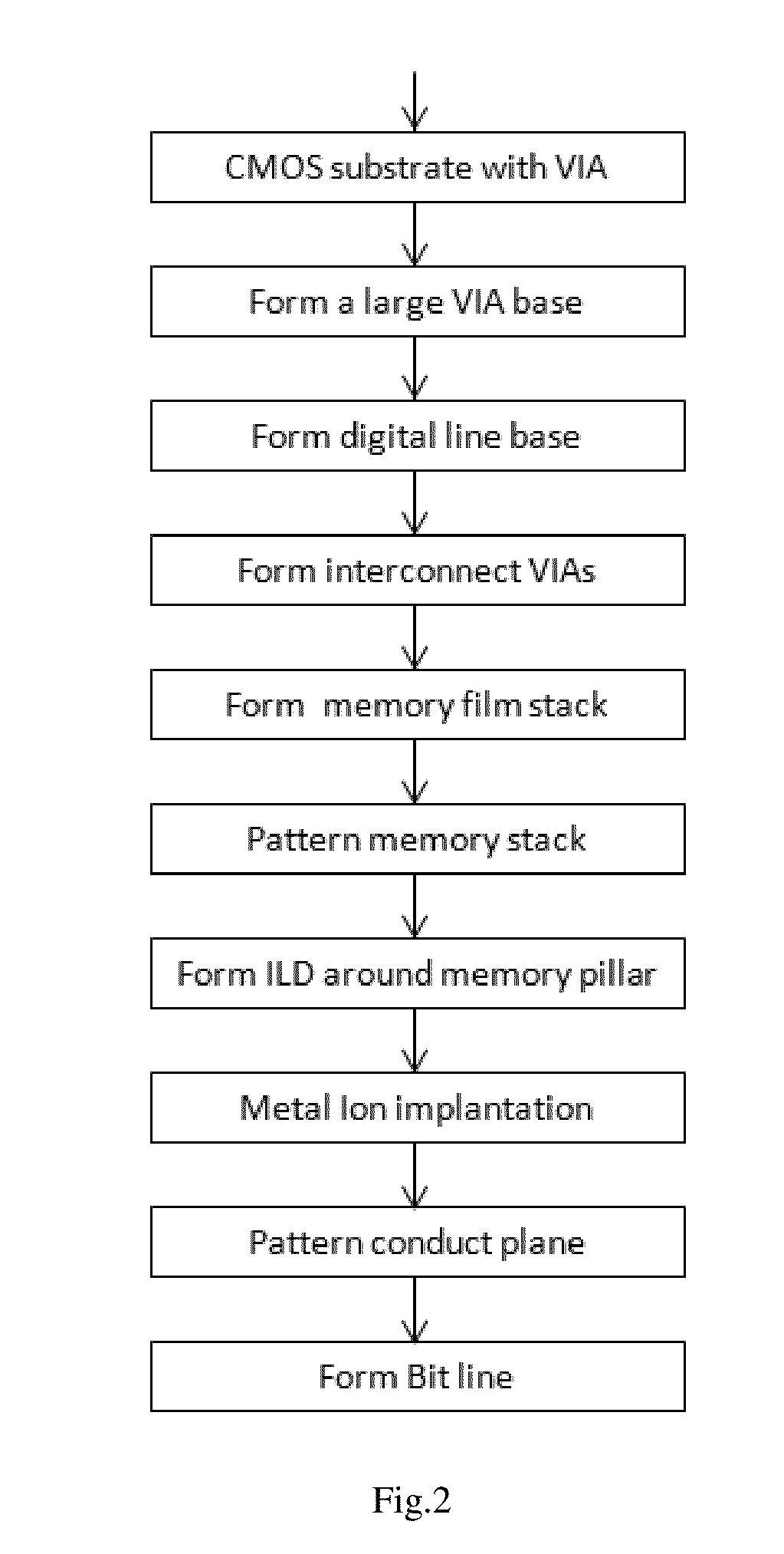
This invention is about a three-terminal spin transistor magnetic random access memory and the method to make it with a narrow foot print. The first terminal, a bit line, is connected to the top magnetic reference layer, and the second terminal is located at the middle memory layer which is connected to the underneath CMOS control circuit through VIA and the third one, a digital line, is a voltage gate with a narrow point underneath the memory layer across an insulating layer which is used to reduce the write current when it is turned on. The fabrication includes formation of a large VIA base, formation of digital line, formation of memory cell & VIA connection and formation of the top bit line. Dual photolithography patterning and hard mask etch are used to form the digital line pillar and small memory pillar. Oxygen plasma ion implantation is used to define an insulating region underneath the memory cell and metallic ion implantation is used to convert a buried dielectric VIA base outside the center memory pillar into an electric conductive path between middle memory cell and underneath CMOS device.

Description

RELATED APPLICATIONS[0001]This application claims the priority benefit of U.S. Provisional Application No. 61 / 834,562 filed on Jun. 13, 2013, which is incorporated herein by reference.BACKGROUND OF THE INVENTION[0002]1. Field of the Invention[0003]This invention relates generally to a three terminal magnetic-random-access memory (MRAM) cell, more particularly to methods of fabricating three terminal MRAM memory elements having ultra-small dimensions.[0004]2. Description of the Related Art[0005]In recent years, magnetic random access memories (hereinafter referred to as MRAMs) using the magnetoresistive effect of ferromagnetic tunnel junctions (also called MTJs) have been drawing increasing attention as the next-generation solid-state nonvolatile memories that can also cope with high-speed reading and writing. A ferromagnetic tunnel junction has a three-layer stack structure formed by stacking a recording layer having a changeable magnetization direction, an insulating tunnel barrier...

Claims


Application Information

Patent Timeline
IPC IPC(8): H01L43/08H01L43/10H01L43/12H01L43/02
CPCH01L43/08H01L43/12H01L43/10H01L43/02H10N50/01H10N50/10
Inventor GUO, YIMIN
Owner T3MEMORY
Learn More