
Soldering method using a low-temperature solder paste

a solder paste and printed circuit board technology, applied in the direction of welding/cutting media/materials, solventing apparatus, manufacturing tools, etc., can solve the problems of low heat resistance electronic parts that cannot be used, pb dissolved in the discarded printed circuit board, and often buried electrical devices, etc., to achieve low heat resistance and reduce electric power consumption

Active Publication Date: 2015-10-01
SENJU METAL IND CO LTD
View PDF34 Cites 2 Cited by
  • Summary
  • Abstract
  • Description
  • Claims
  • Application Information

AI Technical Summary

Benefits of technology

The present invention provides a soldering method that can use a solder composition close to a SnBi eutectic solder for small electronic devices. This method can create a solder joint that has the same resistance to drop impacts as using a traditional solder called SnAgCu, which is currently lead-free. This helps to reduce electric power consumption and use electronic parts with low heat resistance.

Problems solved by technology

However, discarded electrical devices were often buried underground, and Pb dissolved from the discarded printed circuit board and sometimes polluted underground water.
However, as their melting temperature is around 220° C. which is roughly 40° C. higher than that of a conventional Sn—Pb solder, electronic parts having low heat resistance could not be used.
However, it was observed that if these Sn-Bi based solder alloys are used with small electronic devices such as mobile phones or notebook computers, when the small electronic devices are dropped, they have low resistance to drop impacts and fracture at the solder bonding interface.
Therefore, these solder alloys were not used for such electronic devices.

Method used


Image

  • Soldering method using a low-temperature solder paste
  • Soldering method using a low-temperature solder paste
  • Soldering method using a low-temperature solder paste

Examples


example 1

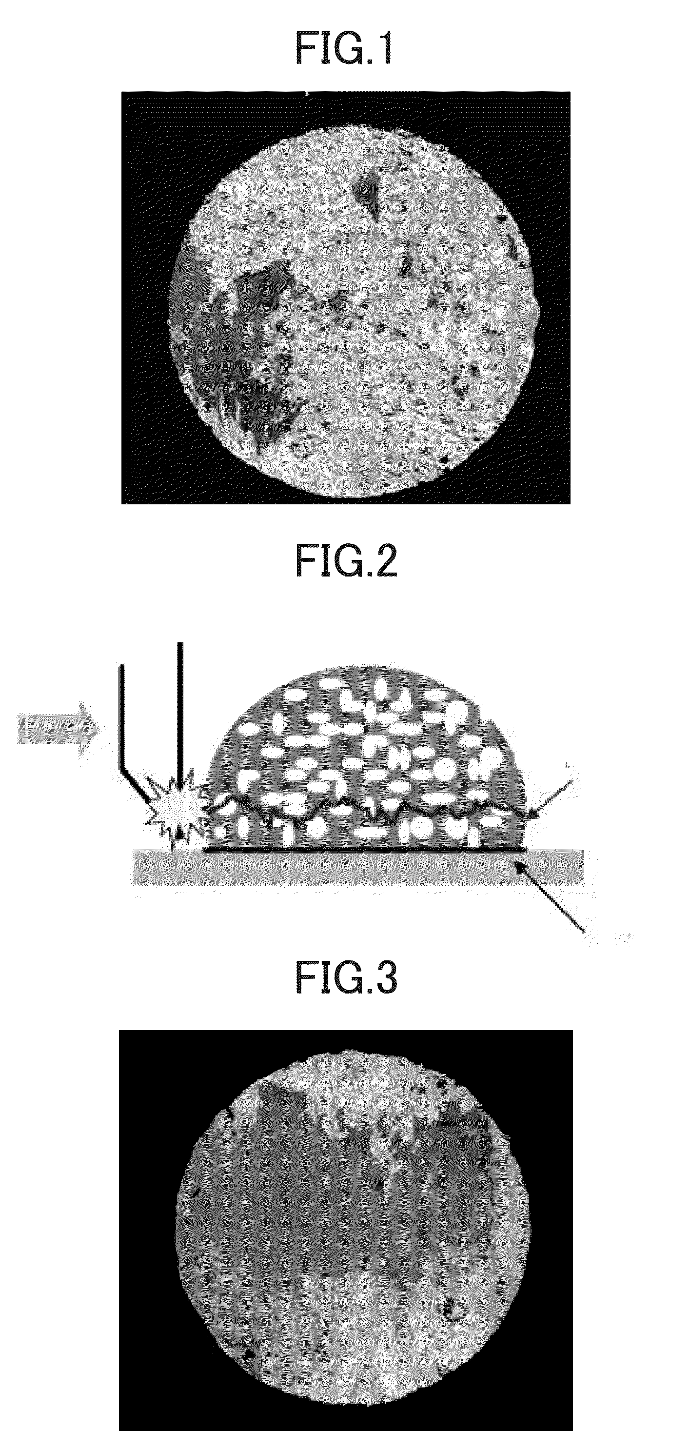
[0034]Under the conditions shown in Table 1, preforms were placed on lands printed with a SnBi-based solder paste, and reflow soldering was carried out under the usual heating conditions for a SnBi-based solder paste.

[0035]After allowing to cool to room temperature, a drop test was carried out, and the number of times until soldered portions broke was measured. The test method for the drop test was as follows. The test board was a glass epoxy printed circuit board (FR-4) measuring 30×120 mm and having a thickness of 0.8 mm.

[0036]In the drop test, both ends of the test board were secured to a special jig with the test board suspended 10 mm above a base. In accordance with JEDEC (Joint Electron Device Engineering Council) specifications, an impact with an acceleration of 1500 G was repeatedly applied. An increase in resistance to at least 1.5 times the initial resistance was viewed as indicating fracture. The number of drops until this level was reached was recorded.

[0037]The results ...

example 2

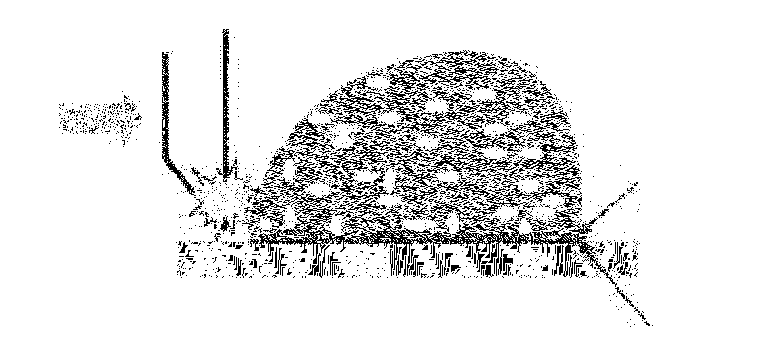
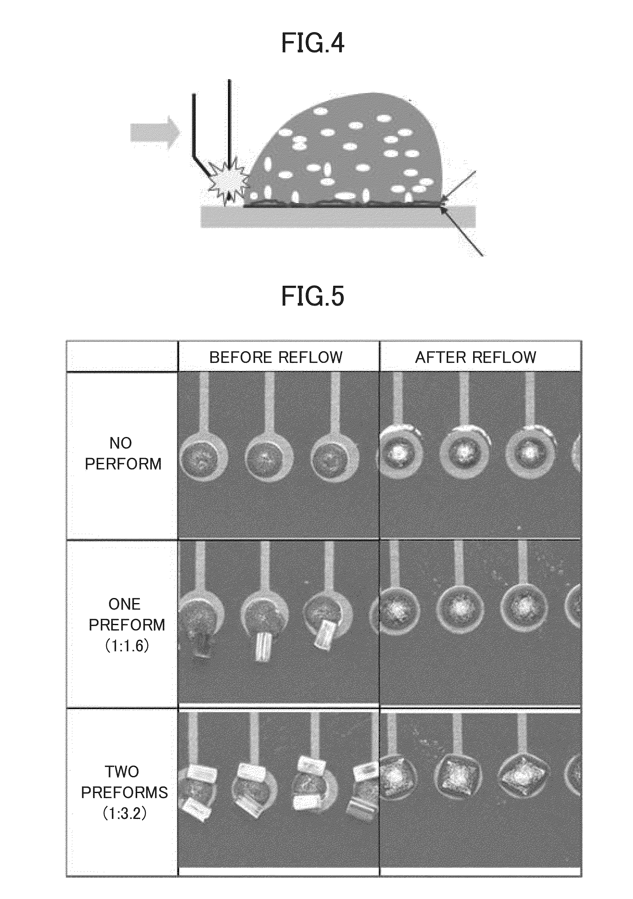
[0040]A solder paste using a solder powder with a Sn-57Bi-1Ag composition was printed onto copper lands measuring 0.5 mm in diameter formed on a printed circuit board like that shown in FIG. 5. One or two preforms having a Sn-3.0Ag-0.5Cu composition and measuring 0.5 mm×0.25 mm were placed atop each land which had been printed with the solder paste, and reflow soldering was carried out at 200° C., which is the usual heating condition for a solder paste with a Sn-57Bi-1Ag solder composition.

[0041]This test ascertained the amount of a preform added to a solder paste of a Sn—Bi composition. With addition of one preform, the ratio of the weight of the solder paste to the weight of the preform was 1:1.6, and with addition of two preforms, it was 1:3.2.

[0042]The soldered state after reflow soldering was observed to ascertain whether it was possible to perform soldering under usual reflow conditions for a low-temperature solder.

[0043]It was confirmed that with one preform, the solder compo...


PUM

PropertyMeasurementUnit
Percent by massaaaaaaaaaa

Abstract

Even if the strength of a solder composition close to a SnBi eutectic composition was improved, it was brittle, so when it was used for small electronic devices such as mobile phones or notebook computers, the resistance to drop impacts when the small electronic equipment was dropped was low. Therefore, interface peeling often took place between the soldered surface and a printed circuit board, resulting in the devices being destroyed. As disclosed, when soldering using a solder paste containing a SnBi-based low-temperature solder, at least one type of solder composition selected from a Sn—Ag, a Sn—Cu, and a Sn—Ag—Cu solder composition is diffused into the solder paste by simultaneously supplying at least one type of preform selected from a Sn—Ag, a Sn—Cu, and a Sn—Ag—Cu solder composition, whereby resistance to drop impacts is improved.

Description

TECHNICAL FIELD[0001]This invention relates to a soldering method for printed circuit boards using a low-temperature solder paste made of a Bi-containing solder and particularly a near-eutectic SnBi solder which is referred to as a low-temperature solder.BACKGROUND ART[0002]The main circuits of electrical devices such as household electrical appliances, audio devices, and computers are printed circuit boards to which electronic parts are soldered. An age ago, a Sn—Pb solder having a composition of Sn-37 mass % Pb (below, % indicates mass %) was used for soldering of printed circuit boards. However, discarded electrical devices were often buried underground, and Pb dissolved from the discarded printed circuit board and sometimes polluted underground water.[0003]In light of this environmental problem, the use of lead-free solders for printed circuit boards has been increasing for more than 10 years, and today, almost all electrical devices are made using lead-free solder.[0004]Convent...

Claims


Application Information

Patent Timeline
IPC IPC(8): H05K3/34C22C12/00B23K35/26C22C13/02B23K1/00B23K35/02
CPCH05K3/3484B23K1/0016B23K35/025B23K35/262H05K2203/12C22C13/02C22C12/00H05K2203/04B23K35/264B23K35/0244B23K35/24B23K35/26B23K35/40H05K3/3463H05K3/3485
Inventor SHIMAMURA, MASATOTACHIBANA, KENHORI, TAKAYUKI
Owner SENJU METAL IND CO LTD
Learn More