Method for manufacturing photo cured material

a technology of photo cured material and manufacturing method, which is applied in the direction of electric/magnetic/electromagnetic heating, circuit masks, instruments, etc., can solve the problem of inability to precisely transfer the convexo-concave pattern of the mold to the resist film, and achieve the effect of improving the transfer precision and small surface roughness

Active Publication Date: 2015-03-19
CANON KK
View PDF4 Cites 15 Cited by
  • Summary
  • Abstract
  • Description
  • Claims
  • Application Information

AI Technical Summary

Benefits of technology

[0011]The present invention can provide a manufacturing method, by which transferring precision can be improved and a photo cured material of small surface roughness can be obtained.
[0012]Further features of the present invention will become apparent from the following description of exemplary embodiments with reference to the attached drawings.

Problems solved by technology

One of the problems to be solved in the photo nanoimprint techniques is how to transfer the convexo-concave pattern of the mold to the resist film precisely.
Thus, air bubbles may remain between the resist film and the mold even after the mold and the resist film comes into contact with, which causes a failure to transfer the convexo-concave pattern of the mold to the resist film precisely.

Method used


Image

  • Method for manufacturing photo cured material
  • Method for manufacturing photo cured material
  • Method for manufacturing photo cured material

Examples


reference example 1

[0110]Firstly, mixed liquid of 4 parts by weight of polystyrene having a molar weight of 96,400 and molecular-weight dispersivity of 1.01 (produced by Polymer Source) and 96 parts by weight of propylene glycol monomethylether acetate (PGMEA, produced by Tokyo Chemical Industry CO., Ltd.) was prepared. Next, the thus prepared mixture liquid was filtered with a 0.2-μm filter made of tetrafluoroethylene, thus obtaining coating liquid.

[0111]Then, drops of this coating liquid were put on a silicon substrate, followed by spin coating at the number of revolutions of 500 rpm for 5 seconds and then of 3,000 rpm for 30 seconds, thus forming a thin film. Then, the thus formed thin film was heated on a hot plate at 90° C. for 90 seconds, whereby the silicon substrate with a polystyrene film formed thereon was obtained.

[0112]A value of surface roughness Peak to Valley (PV) of the thus obtained polystyrene film was measured using an atomic force microscope: Nanoscope produced by Veeco Instruments...

example 1

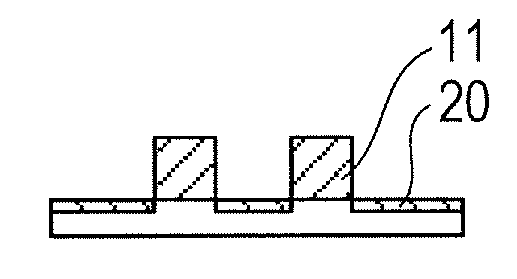
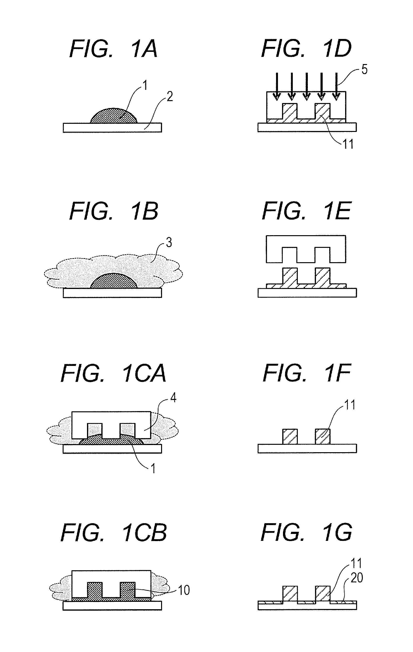
[0117]Commercially-available photo-curable composition PAK-01-60 (produced by Toyo Gosei Co. Ltd.), polystyrene and solvent are mixed, thus obtaining a photo-curable composition. Following the manufacturing processing shown in FIGS. 1A to 1G, the photo-curable composition 1 is applied on the substrate 2 and the photo-curable composition 1 is irradiated with light via the mold 4, whereby a photo cured material having a patterned shape following the convexo-concave pattern on the surface of the mold 4 is obtained.

[0118]While the present invention has been described with reference to exemplary embodiments, it is to be understood that the invention is not limited to the disclosed exemplary embodiments. The scope of the following claims is to be accorded the broadest interpretation so as to encompass all such modifications and equivalent structures and functions.

[0119]This application claims the benefit of Japanese Patent Application No. 2012-102342, filed Apr. 27, 2012, which is hereby ...


PUM

PropertyMeasurementUnit
rate of weight changeaaaaaaaaaa
vapor pressureaaaaaaaaaa
boiling pointaaaaaaaaaa

Abstract

Provided is a method for manufacturing a photo cured material, by which transferring precision can be improved and a small surface roughness can be obtained. The method includes the steps of: placing a photo-curable composition on a substrate; brining a mold into contact with the photo-curable composition; irradiating the photo-curable composition with light; and releasing the mold from the photo-curable composition. The contact is performed in a condensable gas atmosphere, the condensable gas condensing under a temperature condition at the contact and under a pressure condition that the condensable gas receives when the photo-curable composition intrudes gaps between the substrate and the mold or concavities provided on the mold, and the photo-curable composition includes a gas dissolution inhibitor having a rate of weight change with reference to the condensable gas that is −1.0% to 3.0%.

Description

TECHNICAL FIELD[0001]The present invention relates to a method for manufacturing a photo cured material, particularly a photo cured material having a predetermined patterned shape.BACKGROUND ART[0002]A photo nanoimprint is available as a technique to process a resin material in a nanometer scale or to fabricate a resin film having a nano-scale pattern.[0003]The photo nanoimprint technique uses a mold, on a surface of which a minute convexo-concave pattern is formed, to make a resin material / resin film having a patterned shape following this minute convexo-concave pattern. More specifically, the photo nanoimprint technique is to form / process a resin film where the mold is pressed against a substrate with resist (photo-curable composition) applied thereon and the resist is irradiated with light via the mold for curing, whereby the convexo-concave pattern of the mold is transferred to the resist film on the substrate.[0004]One of the problems to be solved in the photo nanoimprint techn...

Claims


Application Information

Patent Timeline
Patent Type & Authority Applications(United States)
IPC IPC(8): B29C35/08C08F112/08H05K3/00H05K3/06B29C59/02H05K1/18
CPCB29C35/0805B29C59/022H05K1/181H05K3/0082H05K3/064B29K2995/0027B29C2035/0827B29K2025/06B29K2025/08B29K2105/0002B29K2105/0085C08F112/08G03F7/0002H01L21/0273B29C59/02B29C59/021H01L21/027
Inventor ITO, TOSHIKIIIMURA, AKIKO
Owner CANON KK
Why Eureka
Try Eureka