Crystallization substrate, crystallization container, crystallization device, and crystal producing method
a crystallization device and substrate technology, applied in the field of crystallization substrates, crystallization containers, crystallization devices, etc., can solve the problems of poor repeatability, large quantities of high-concentration polymer samples, and skilled operation, and achieve the effect of efficient production
- Summary
- Abstract
- Description
- Claims
- Application Information
AI Technical Summary
Benefits of technology
Problems solved by technology
Method used
Image
Examples
example 1
Substrate Fabrication
[0176]A gold thin film (average thickness 40 nm) was vapor deposited on one surface of cover glass (diameter 22 mm, thickness 0.2 mm) under 99.99% gold purity and 10−1 Pa vacuum conditions, using an ion sputtering device JFC-1500 (vapor deposition device available from JEOL).
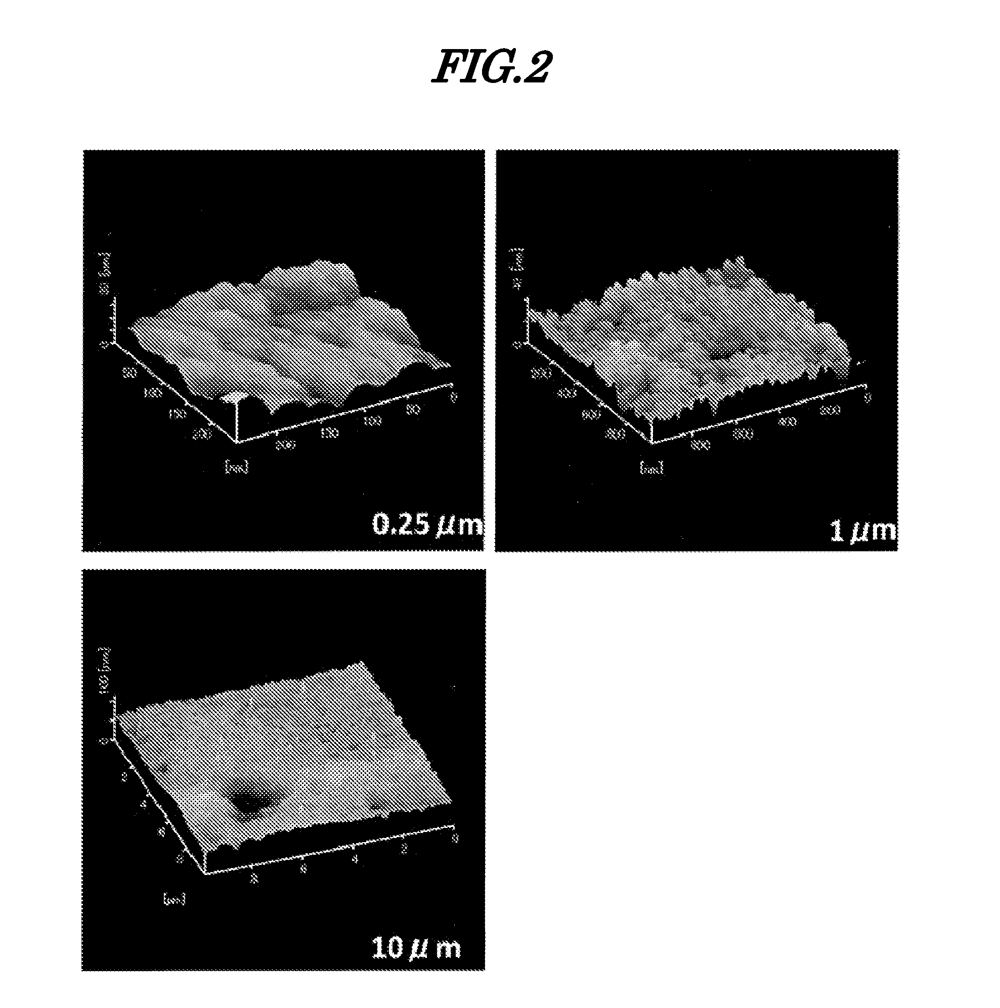
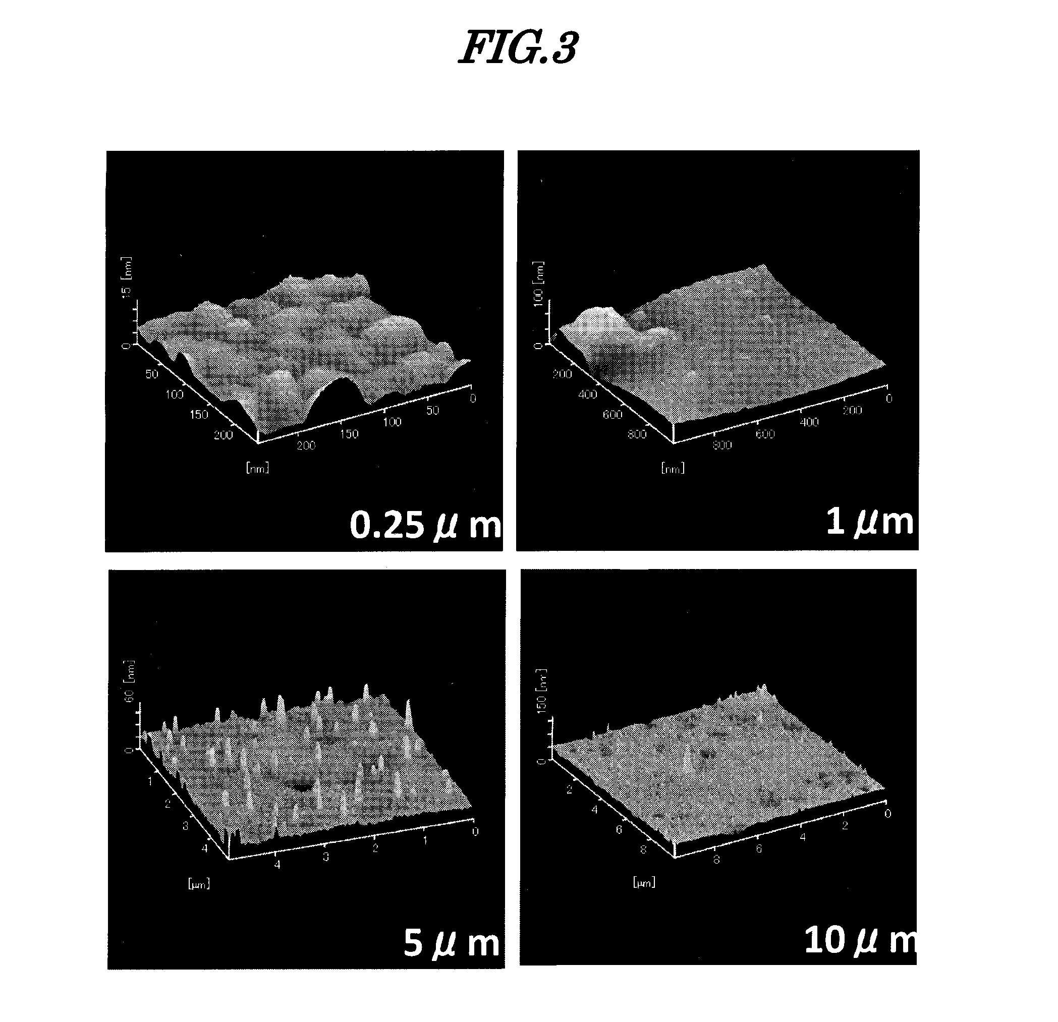
[0177]Atomic force microscopy (S-weep spi3800; Seiko Instruments Inc.) of the cover glass revealed the presence of pits in the gold thin film of the cover glass.
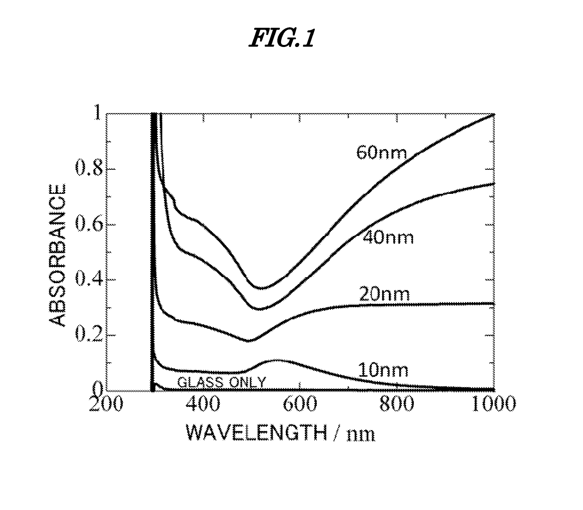
[0178]The absorption spectrum of the gold thin film on the cover glass was measured with a spectrophotometer U-2100 (Hitachi High-Technologies). The gold thin film had an absorption in the whole 500 to 1,000 nm wavelength range. The absorbance at 600 nm wavelength was 0.38.
[0179]A 50 mM sodium acetate buffer solution with a pH 4.3 containing 15 mg / mL of chicken egg white lysozyme, and 0.7 M sodium chloride was used as a protein solution.
[0180]10 μl of the protein solution was dropped onto the cover glass ...
example 2
[0186]Substrate fabrication, and biopolymer crystallization were performed in the same manner as in Example 1, except that the gold thin film was vapor deposited to make the average thickness 20 nm. The results are presented in Table 1.
[0187]Atomic force microscopy of the cover glass revealed the presence of pits in the gold thin film of the cover glass.
[0188]The absorption spectrum of the gold thin film on the cover glass was measured with the spectrophotometer. The gold thin film had an absorption in the whole 500 to 1,000 nm wavelength range. The absorbance at 600 nm wavelength was 0.28.
example 3
[0189]Substrate fabrication, and biopolymer crystallization were performed in the same manner as in Example 1, except that the gold thin film was vapor deposited to make the average thickness 10 nm. The results are presented in Table 1.
[0190]Atomic force microscopy of the cover glass revealed the presence of pits in the gold thin film of the cover glass.
[0191]The absorption spectrum of the gold thin film on the cover glass was measured with the spectrophotometer. The gold thin film had an absorption in the whole 500 to 1,000 nm wavelength range. The absorbance at 600 nm wavelength was 0.09. The absorbance at 1,000 nm wavelength was 0.005 or higher.
PUM
| Property | Measurement | Unit |
|---|---|---|
| wavelength range | aaaaa | aaaaa |
| thickness | aaaaa | aaaaa |
| thickness | aaaaa | aaaaa |
Abstract
Description
Claims
Application Information
 - R&D
- Intellectual Property
- Life Sciences
- Materials
- Tech Scout
- Unparalleled Data Quality
- Higher Quality Content
- 60% Fewer Hallucinations
Browse by: Latest US Patents, China's latest patents, Technical Efficacy Thesaurus, Application Domain, Technology Topic, Popular Technical Reports.
© 2025 PatSnap. All rights reserved.Legal|Privacy policy|Modern Slavery Act Transparency Statement|Sitemap|About US| Contact US: help@patsnap.com


