
Stacked diode limiter

a diode limiter and diode technology, applied in the direction of diodes, waveguides, electrical equipment, etc., can solve the problems of interference signal flowing into the in-band communication frequency band that cannot be eliminated using only a filtering method, physical damage or malfunction of the connected to the subsequent stage of the antenna,

Active Publication Date: 2015-01-01
ELECTRONICS & TELECOMM RES INST
View PDF9 Cites 8 Cited by
  • Summary
  • Abstract
  • Description
  • Claims
  • Application Information

AI Technical Summary

Benefits of technology

The present invention is aimed at providing a stacked diode limiter that can protect wireless systems from malicious high-power electromagnetic pulse signals and Intentional Electromagnetic Interference (IEMI) signals that may include a power of several thousand W or more. The invention suppresses and eliminates these signals that can cause damage to wireless devices. Its specific technical effect is to enhance the security and reliability of wireless systems against malicious signals.

Problems solved by technology

However, when an interference pulse signal source, the frequency band of which is identical to that of the in-band communication frequency band, or the frequency band of which includes a part of the corresponding frequency band and which has a peak power of several hundreds of W to several tens of kW, is input to a wireless communication system through the antenna, a semiconductor device (in particular, the transistor part of a low-noise amplifier) connected to the subsequent stage of the antenna may be physically damaged or may malfunction (or be disordered) at such a predetermined power intensity or more.
An interference signal flowing into an in-band communication frequency band cannot be eliminated using only a filtering method.
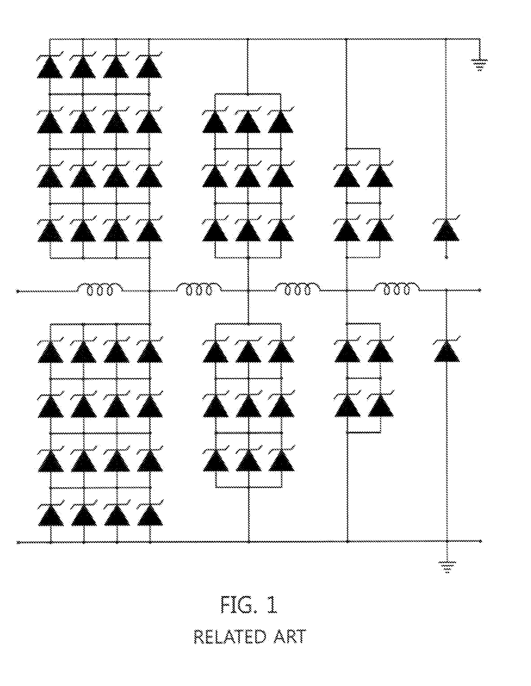
Generally, a modular limiter device used in the antenna line of a wireless communication system or the like has a structure in which surface-mount diodes (SMD) are assembled on a planar board, and is typically operated within the range of input power of several tens of W. If the input power of the modular limiter device increases to several kW or more, an interval between the signal line of a microstrip line and a bottom ground layer is decreased, thus causing an electrical breakdown phenomenon.
Further, when discharge caused by the electrical breakdown is continued, the board may be burned out or the conductor of a signal line may be melted.
However, such a waveguide structure is also disadvantageous in that when the frequency is decreased below several hundreds of MHz to several GHz, the size of the aperture of the waveguide is increased, and then the arrangement of the waveguide-type transmission line in the system is limited.
The structure of U.S. Pat. No. 6,853,264 is limited to the use of Schottky diodes without using PIN diodes typically used as limiter diodes.
The reason for this is that it is impossible to integrate PIN diodes using the same process as that of a low-noise amplifier chip manufactured using a GaAs semiconductor process.
In a semiconductor chip process, if ¼ wavelength is made using the length of only the microstrip line, the transmission line is excessively lengthened, so that the manufacture cost of chips is greatly increased, and thus inductors are employed as a method of compensating for an increase in the length of the line.
However, when such diodes are coupled to each other using inductors, high inductance occurs compared to the transmission line and high-frequency characteristics are limited, and thus there is a disadvantage in that a usable frequency band may be restricted.
Further, due to the operating power limits of Schottky diodes (having an input power limit of a total of 1 W or less) used for integration in a GaAs chip manufacturing process, even if a plurality of diodes are arranged in series and in parallel, the number of diodes that must be connected may reach several tens to several hundreds so as to operate even at pulse power of kW levels, thus greatly deviating from the original purpose of the limiter, that is, a previous stage protection circuit used in small-sized chips.
Further, a problem may arise in that, as the number of array diodes increases, the floating inductance and the floating capacitance of the circuit are continuously increased, and high-frequency impedance and insertion loss performance may be deteriorated, thus causing the use of the corresponding circuit to be greatly restricted.

Method used


Image

  • Stacked diode limiter
  • Stacked diode limiter
  • Stacked diode limiter

Examples


Embodiment Construction

[0043]Hereinafter, a stacked diode limiter according to embodiments of the present invention will be described in detail with reference to the attached drawings. Prior to the detailed description of the present invention, it should be noted that the terms or words used in the present specification and the accompanying claims should not be limitedly interpreted as having their common meanings or those found in dictionaries. Therefore, the embodiments described in the present specification and constructions shown in the drawings are only the most preferable embodiments of the present invention, and are not representative of the entire technical spirit of the present invention. Accordingly, It should be understood that various equivalents and modifications capable of replacing the embodiments and constructions of the present invention might be present at the time at which the present invention was filed.

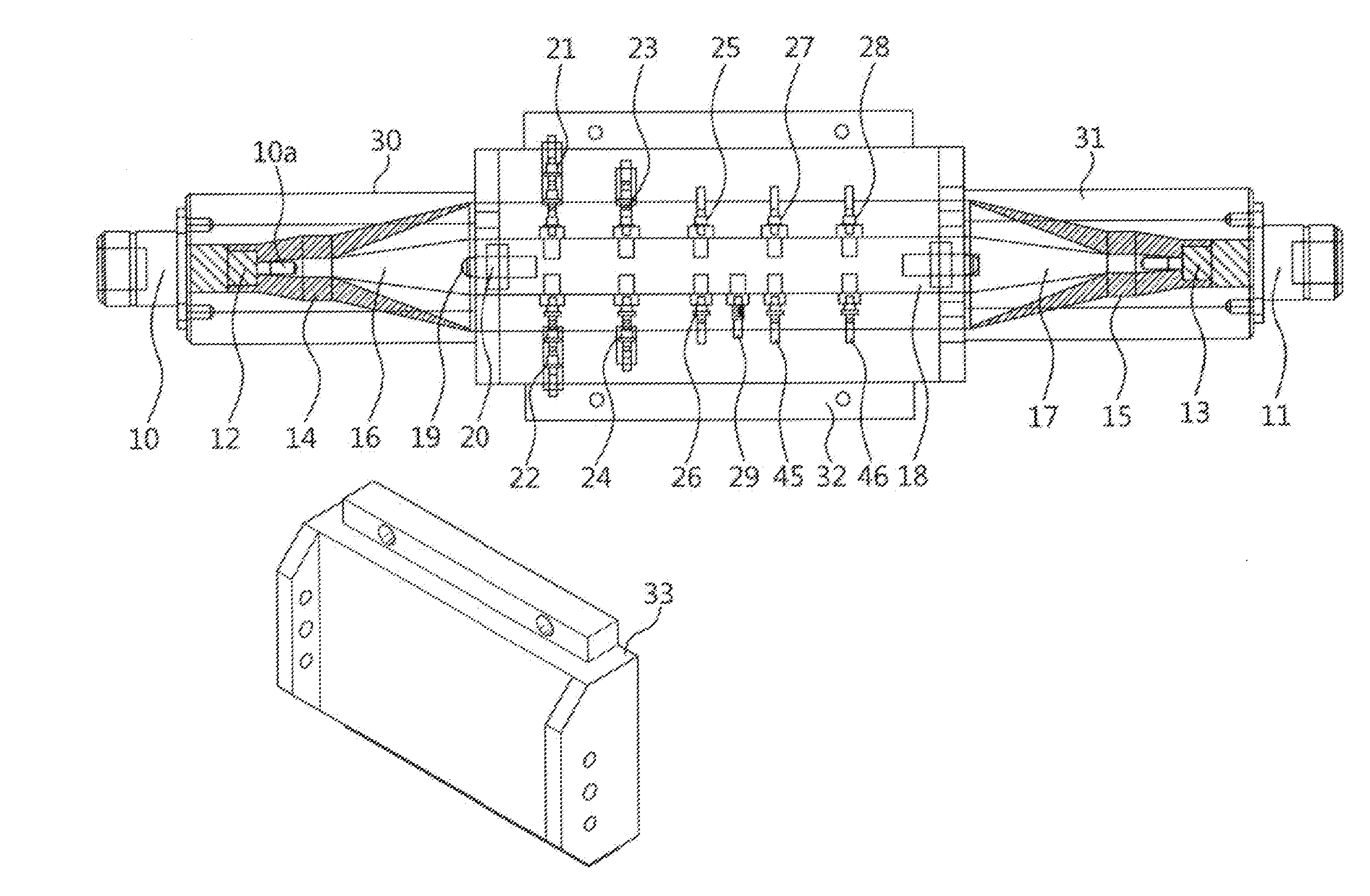
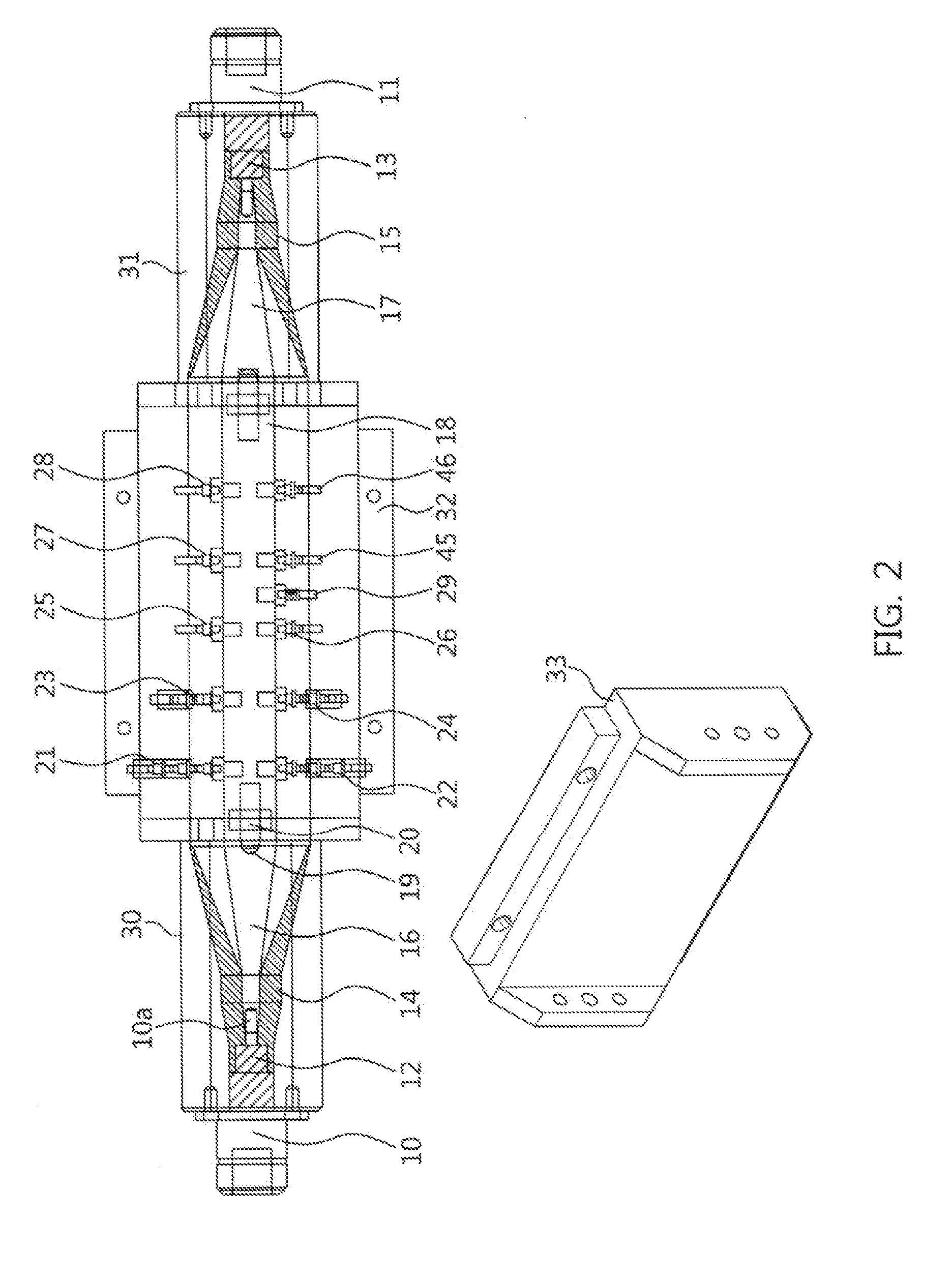
[0044]FIG. 2 is a diagram showing the configuration of a stacked diode limiter acco...


PUM


Abstract

A stacked diode limiter, which can suppress and eliminate a malicious high-power electromagnetic pulse signal and an Intentional Electromagnetic Interference (IEMI) signal that are input to the antenna line of a wireless system and that include a communication service frequency component having a power of several kW or more, includes a stacked diode unit including one or more diode stack parts formed on a center electrode of a coaxial line formed between an input connector and an output connector, each diode stack part being configured such that a plurality of diodes are arranged in series and stacked on top of one another, and an impedance matching unit for configuring dielectrics between the connectors and the coaxial line as heterogeneous dielectrics and matching impedances between the connectors and the coaxial line.

Description

CROSS REFERENCE TO RELATED APPLICATION[0001]This application claims the benefit of Korean Patent Application No. 10-2033-0074674 filed on Jun. 27, 2033, which is hereby incorporated by reference in its entirety into this application.BACKGROUND OF THE INVENTION[0002]1. Technical Field[0003]The present invention relates generally to a stacked diode limiter and, more particularly, to a stacked diode limiter, which reduces the power intensity of a high-power interference pulse input to an in-band communication frequency band, thus protecting an electronic device arranged at the subsequent stage of an antenna in a wireless system.[0004]2. Description of the Related Art[0005]In the case of an operating frequency band of a wireless communication system, only signals in a specific band are transmitted without loss by a filter at an input stage and frequency signals out of the band are sufficiently attenuated by the filter.[0006]However, when an interference pulse signal source, the frequenc...

Claims


Application Information

Patent Timeline
IPC IPC(8): H03G11/00
CPCH01P1/222H01P1/005H01P1/202H01P1/225H03G11/02H01P3/06
Inventor RYU, SEUNG-KABLEE, KYUNG-HOONCHU, KWANG-UKKIM, UIJUNGNAMKOONG, UP
Owner ELECTRONICS & TELECOMM RES INST
Learn More