Piezoelectric device
a technology of piezoelectric film and piezoelectric force, which is applied in piezoelectric/electrostrictive/magnetostrictive devices, piezoelectric/electrostriction/magnetostriction machines, electrical apparatus, etc., can solve the problems of large displacement, low reliability, and small displacement of piezoelectric film, and achieves high reliability, large displacement, and low cost.
- Summary
- Abstract
- Description
- Claims
- Application Information
AI Technical Summary
Benefits of technology
Problems solved by technology
Method used
Image
Examples
example 1
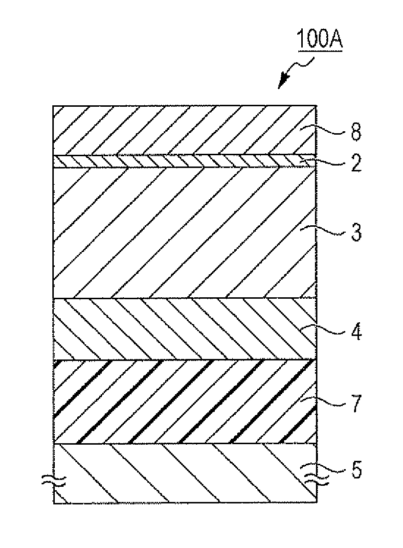
Piezoelectric Device 100A
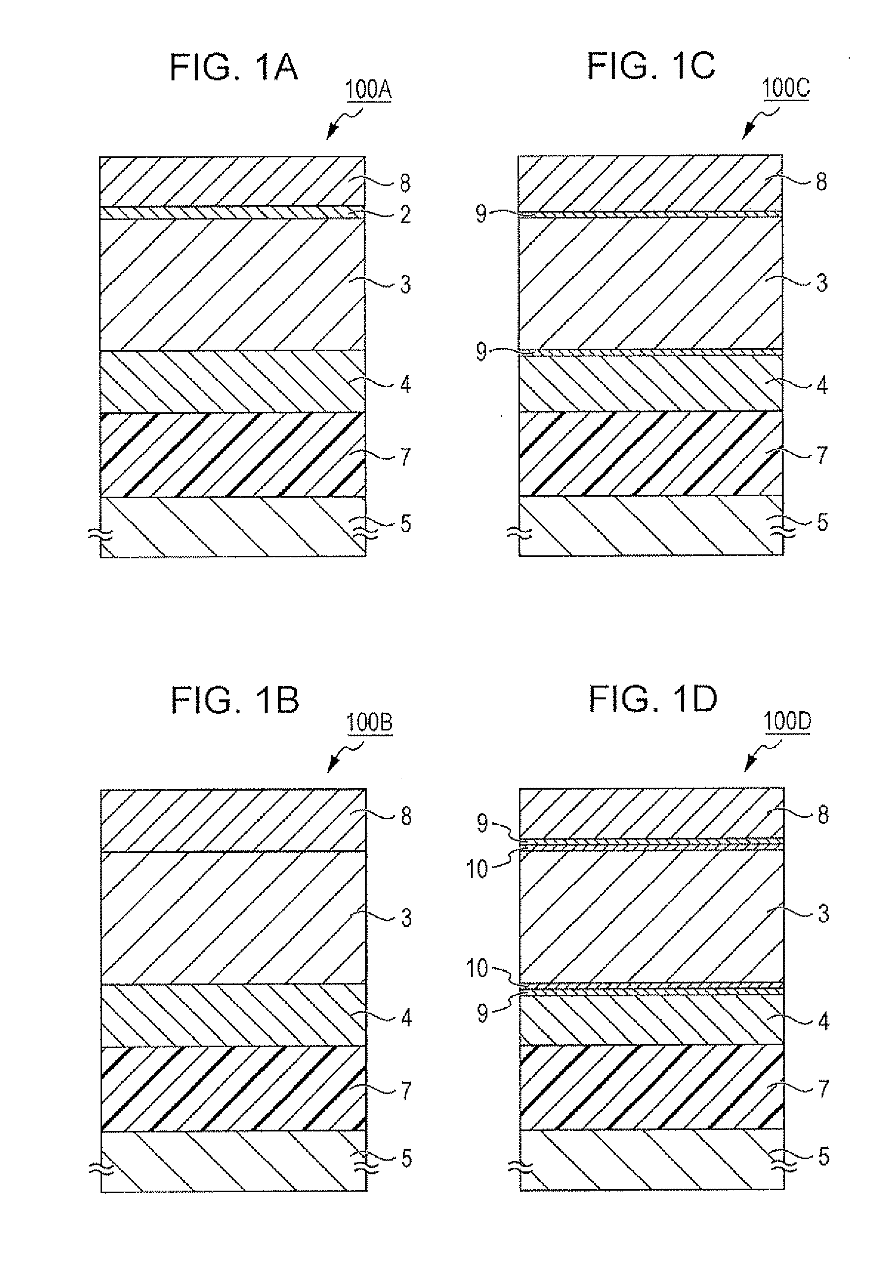
[0086]As shown in FIG. 1A, a metal film 2 having a (100) preferential orientation was formed on a silicon substrate 1 by epitaxially growing a Pt film having a thickness of 50 nm on a silicon substrate. A piezoelectric film 3 having a thickness of 2000 nm was formed on the Pt film by sputtering that uses a potassium sodium niobate (KNN) target substrate. An electrode film 4 composed of Zn—Al was formed on the piezoelectric film 3, and the electrode film 4 was bonded to a silicon support substrate 5 through an epoxy resin layer 7. Subsequently, the silicon substrate 1 was removed from the metal film 2 by RIE. A Zn—Al alloy film (having the same composition as that of the electrode film 4) having a thickness of 200 nm was formed on the metal film 2 by sputtering at room temperature and thus an amorphous electrode film 8 was formed. As a result, a piezoelectric device 100A was obtained. Note that the composition of the KNN target substrate was adjusted so that ...
example 2
Piezoelectric Device 100B
[0087]A piezoelectric device 100B was produced in the same manner as in Example 1, except that the metal film 2 was also removed by etching when the silicon substrate 1 was removed.
example 3
Piezoelectric Device 100C
[0088]A piezoelectric device 100C was produced in the same manner as in Example 2, except that an intermediate film 9 composed of Ti and having a non-oriented structure was formed by sputtering between the piezoelectric film 3 and the electrode films 4 and 8 so as to have a thickness of 5 nm. Thus, the adhesiveness between the piezoelectric film 3 and the electrode film 4 and between the piezoelectric film 3 and the electrode film 8 was improved.
PUM
| Property | Measurement | Unit |
|---|---|---|
| oxidation-reduction potential | aaaaa | aaaaa |
| oxidation-reduction potentials | aaaaa | aaaaa |
| piezoelectric | aaaaa | aaaaa |
Abstract
Description
Claims
Application Information
 - R&D
- Intellectual Property
- Life Sciences
- Materials
- Tech Scout
- Unparalleled Data Quality
- Higher Quality Content
- 60% Fewer Hallucinations
Browse by: Latest US Patents, China's latest patents, Technical Efficacy Thesaurus, Application Domain, Technology Topic, Popular Technical Reports.
© 2025 PatSnap. All rights reserved.Legal|Privacy policy|Modern Slavery Act Transparency Statement|Sitemap|About US| Contact US: help@patsnap.com


