
Composition for hardmask, method of forming patterns using the same, and semiconductor integrated circuit device including the patterns

a technology of semiconductor integrated circuits and hardmasks, applied in the direction of originals for photomechanical treatment, photomechanical devices, instruments, etc., can solve the problem of ineffective transfer of predetermined patterns, and achieve excellent etching resistance and anti-reflective properties

Active Publication Date: 2014-11-13
CHEIL IND INC
View PDF1 Cites 2 Cited by
  • Summary
  • Abstract
  • Description
  • Claims
  • Application Information

AI Technical Summary

Benefits of technology

This patent text describes a composition for a hardmask that has excellent etching resistance and antireflective properties. The composition includes a copolymer that has repeating units represented by a specific chemical formula. The composition can be used in various applications, such as semiconductor device manufacturing, to provide high-quality etching results and reduce reflective light during the manufacturing process.

Problems solved by technology

However, in some lithographic imagification processes, the used resist does not provide an enough resistance for the subsequent etching step so that a predetermined pattern is not effectively transferred to the layer on the back surface.

Method used


Image

  • Composition for hardmask, method of forming patterns using the same, and semiconductor integrated circuit device including the patterns
  • Composition for hardmask, method of forming patterns using the same, and semiconductor integrated circuit device including the patterns
  • Composition for hardmask, method of forming patterns using the same, and semiconductor integrated circuit device including the patterns

Examples


synthesis example 1-1

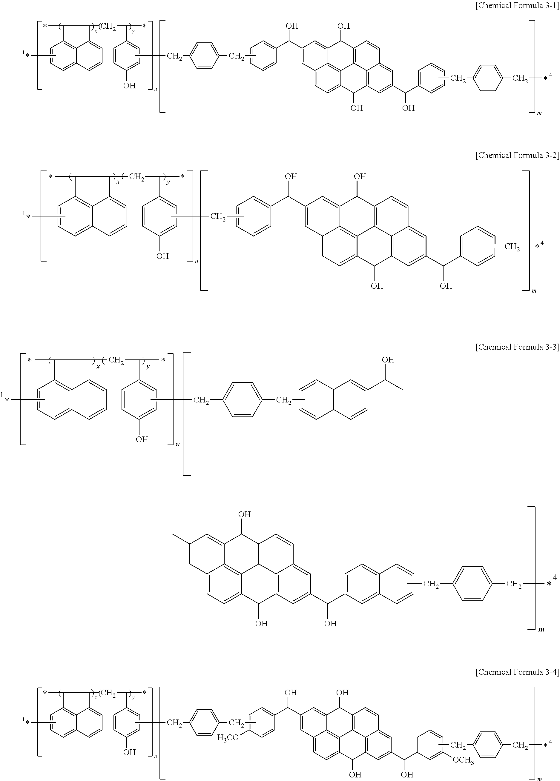
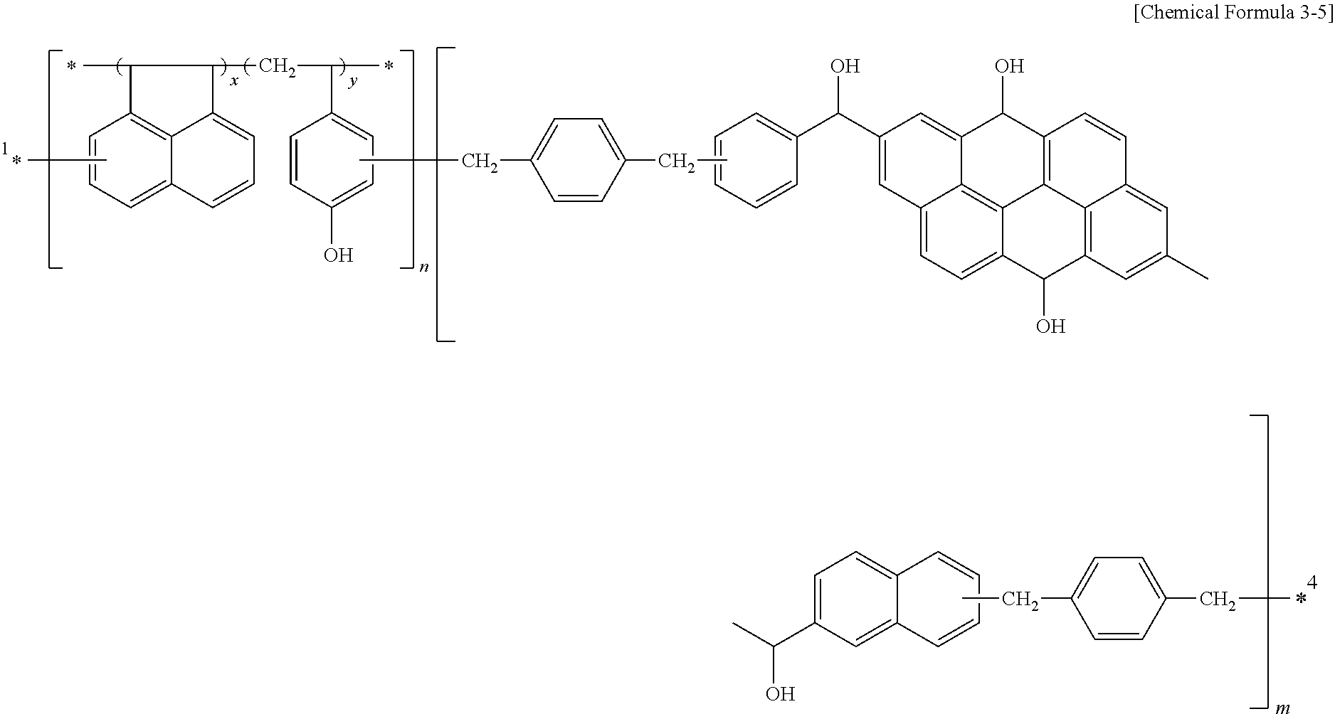
[0087]30.6 g (100 mmol) of anthanthrone represented as a compound A in the following reaction scheme 1, 28 g (200 mmol) of benzoyl chloride, and 306 g of dichloroethane were put in a flask and dissolved. Next, 26.7 g (200 mmol) of aluminum (III) chloride was slowly added thereto, and the mixture was heated up to 80° C. and agitated for 24 hours. When the reaction was complete, the reactant was cooled down to room temperature, and a potassium hydroxide aqueous solution was added thereto for neutralization. Then, an organic layer was separated from the resulting product, and the remaining solution was concentrated, obtaining 48.3 g (a yield of 94.0%) of a compound B.

[0088]51.4 g (100 mmol) of the compound B was dissolved in 514 g of an aqueous solution prepared by mixing methanol and water in a weight ratio of 1:1. Next, 38.83 g (1.0 mol) of sodium borohydride was slowly added to the solution, and the mixture was agitated for 24 hours. When the reaction was complete, a 10% HCl aqueous...

synthesis example 1-2

[0089]The following monomer D (a yield of 76%) was synthesized according to the same method as Synthesis Example 1-1 except for using naphtoyl chloride instead of benzoyl chloride.

synthesis example 1-3

[0090]The following monomer E (yield 83%) was synthesized according to the same method as Synthesis Example 1-1 except for using 4-methoxybenzoyl chloride instead of benzoyl chloride.


PUM

PropertyMeasurementUnit
temperatureaaaaaaaaaa
volume ratioaaaaaaaaaa

Abstract

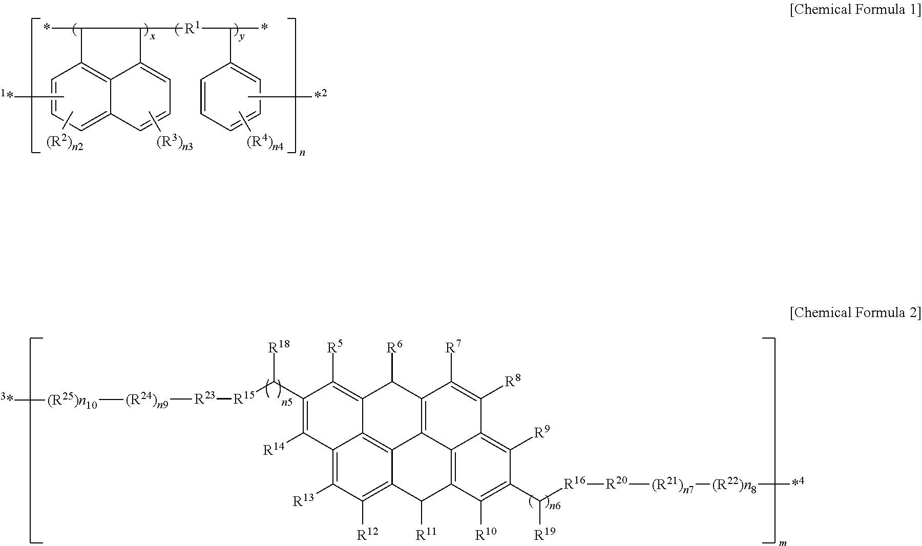
A composition for a hardmask including copolymer including repeating units represented by Chemical Formulae 1 and 2 and a solvent, a method of forming a pattern using the same, and a semiconductor integrated circuit device including a pattern formed using the method are provided.

Description

TECHNICAL FIELD[0001]A composition for a hardmask, a method of forming a pattern using the same, and a semiconductor integrated circuit device including the pattern are disclosed.BACKGROUND ART[0002]In the industrial fields of, for example, fabricating a microscopic structure (e.g., a micromachine, a magneto-resist head, and the like) as well as microelectronics, it is required to provide a number of circuits more than expected in the provided chip size by decreasing the pattern size. Effective lithographic techniques are essential to achieve a reduction in the size of structural shapes. Lithography affects on fabricating a microscopic structure in the views of directly imagining a pattern on a predetermined substrate and of providing a mask typically used for the imagification.[0003]A typical lithographic process involves the following processes. First, a radiation-sensitive resist is exposed in patternwise method to form a patterned resist layer. Subsequently, the exposed resist l...

Claims


Application Information

Patent Timeline
Patent Type & Authority Applications(United States)
IPC IPC(8): G03F1/00G03F7/20
CPCG03F1/00G03F7/20G03F7/09G03F7/40G03F7/004G03F7/11G03F7/26G03F7/265H01L21/0273G03F7/091H01L21/0276H01L21/0332G03F7/0752G03F7/094
Inventor LEE, SUNG-JAEMOON, JOON-YOUNGCHO, YOUN-JINKIM, YOUNG-MINYOON, YONG-WOON
Owner CHEIL IND INC
Learn More