High throughput epitaxial deposition system for single crystal solar devices

a solar device and high-throughput technology, applied in the direction of polycrystalline material growth, crystal growth process, chemically reactive gas, etc., can solve the problems of poor uniformity, low throughput, and high gas consumption, so as to improve the use of process gases, reduce the effect of unwanted deposition and high throughpu

Inactive Publication Date: 2014-10-30
CRYSTAL SOLAR INC
View PDF4 Cites 9 Cited by
  • Summary
  • Abstract
  • Description
  • Claims
  • Application Information

AI Technical Summary

Benefits of technology

The present invention provides an improved design for an epitaxial reactor with higher throughput, a wafer sleeve containing a multiplicity of wafers within a small reaction volume to improve usage of process gases and minimize unwanted deposition on the reaction chamber walls, increased lamp lifetimes through improved lamp temperature control, and a method of lamp sequencing to further enhance film deposition uniformities. The epitaxial reactor may be integrated within a system comprising a preheat chamber, a single epitaxial deposition reactor, and a cool down chamber, or multiple epitaxial reactors in series with a preheat chamber and cool down chamber. The wafer sleeve is heated by an array of lamps, and a method of lamp sequencing can be employed to control the deposition rate through real-time control of the wafer temperatures in different parts of the wafer sleeve. The substrates can be mounted in the wafer sleeat an angle to compensate for TCS gas depletion.

Problems solved by technology

Key disadvantages of this type of epitaxial reactor are low throughput, high gas consumption, wafer warpage, and worse uniformities than other types of prior art epitaxial reactors (see FIGS. 2 and 3).
Another important disadvantage is the need for frequent cleaning of the inner surfaces of the reactor chamber 101 due to unwanted deposition of films on these surfaces.
This unwanted deposition increases the cost of ownership due to higher process gas consumption and increased system downtime for maintenance and cleaning.
Some disadvantages are an inability to deposit dual layers and relatively high film resistivities.
However, an important disadvantage of this type of reactor is the high film costs for thicker films where the throughputs drop due to the longer epitaxial deposition times required.
Thus, the economics of semiconductor manufacturing may support relatively higher costs for each processing step than would be the case for other types of semiconductor products such as photovoltaic (PV) solar cell wafers.
Epitaxial deposition of a thin-film solar cell has the disadvantage that epitaxial deposition is typically a relatively slow process in achieving good epitaxy but the semiconducting light absorbing layers in a solar cell need to be relatively thick.

Method used


Image

  • High throughput epitaxial deposition system for single crystal solar devices
  • High throughput epitaxial deposition system for single crystal solar devices
  • High throughput epitaxial deposition system for single crystal solar devices

Examples


Embodiment Construction

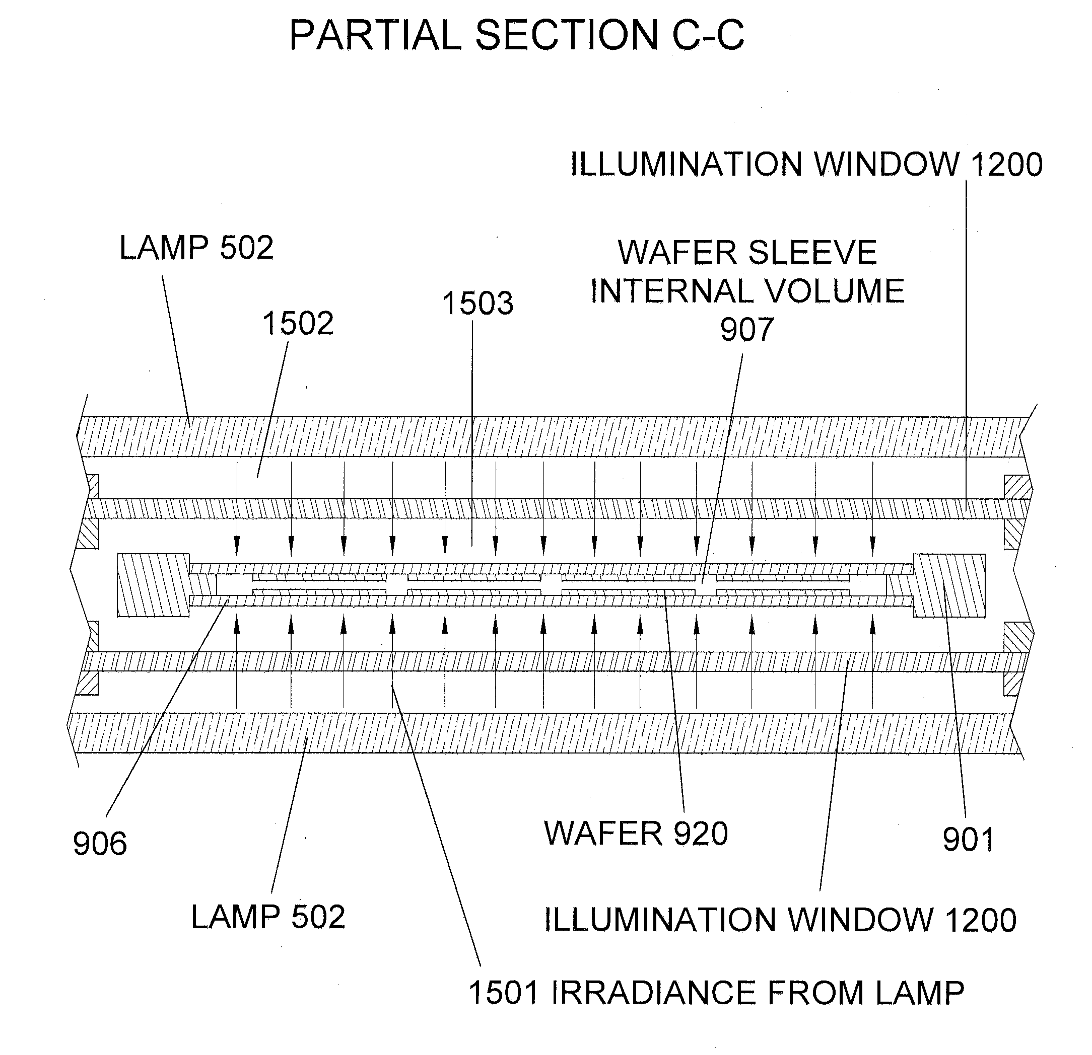
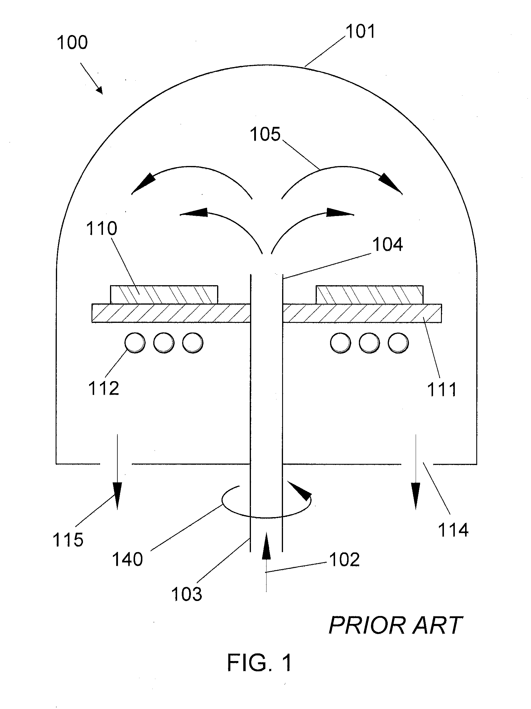
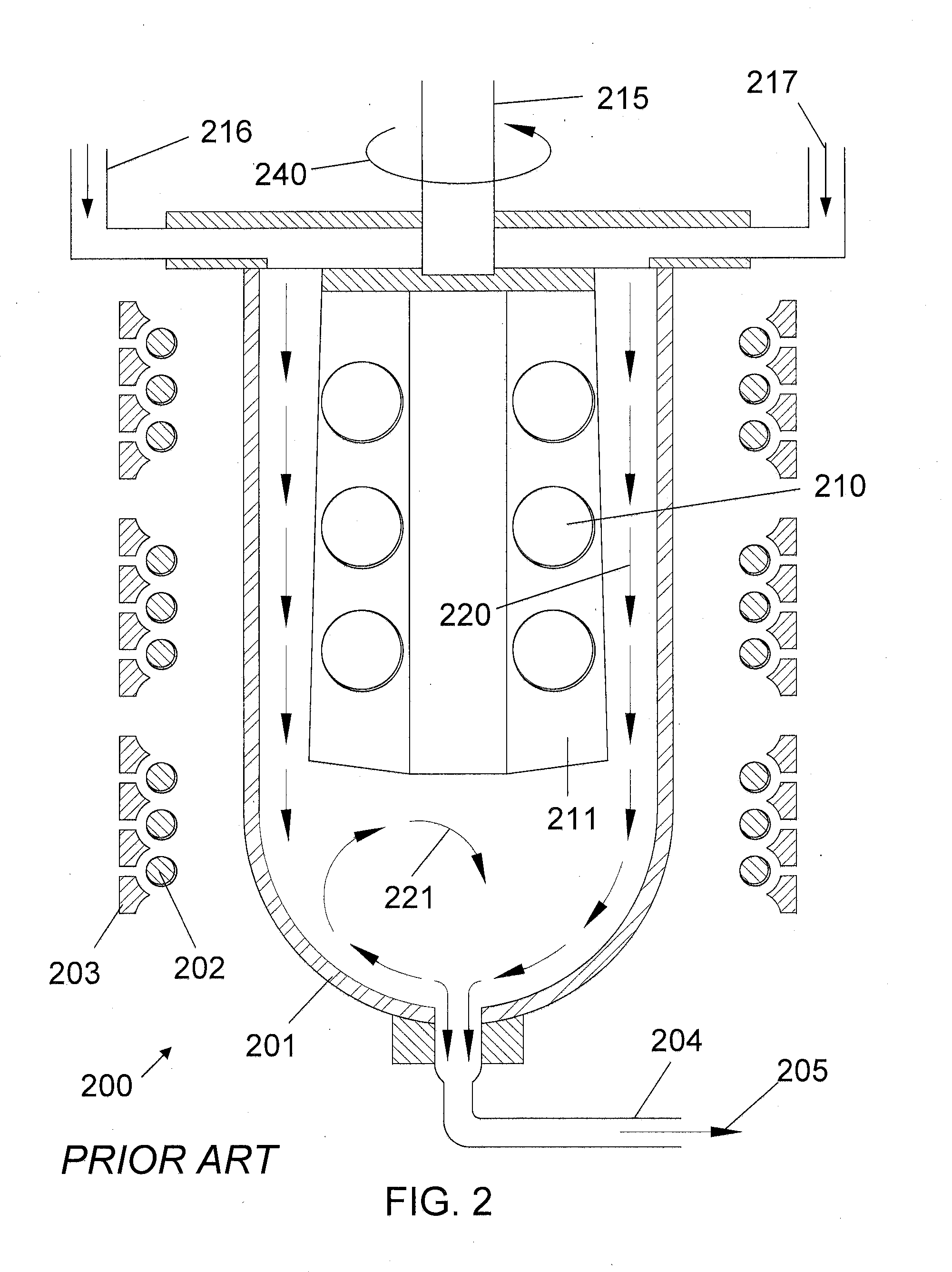
[0063]One disadvantage of prior art epitaxial deposition systems for PV cell applications is low throughput, measured in wafers per hour. Thus, it would be desirable for an epitaxial reactor to process a large number of wafers in parallel with the minimum deposition time practical to still achieve the desired properties in the deposited films on PV solar cell wafers.

[0064]Accordingly, one aspect of the present invention includes an epitaxial reactor enabling the simultaneous deposition by chemical vapor deposition of films on a multiplicity of wafers, each supported by a carrier plate heated by an array of lamps mounted within a reflector assembly. The epitaxial reactor of the present invention comprises one or more lamp modules which irradiate a wafer sleeve contained within a reactor frame which also supports the lamp modules. The following figures describe the lamp module, wafer sleeve, and reactor frame separately. Next, the assembly of a reactor module is described, followed by...


PUM

PropertyMeasurementUnit
angleaaaaaaaaaa
diameteraaaaaaaaaa
diameteraaaaaaaaaa

Abstract

An epitaxial reactor enabling simultaneous deposition of thin films on a multiplicity of wafers is disclosed. During deposition, a number of wafers are contained within a wafer sleeve comprising a number of wafer carrier plates spaced closely apart. Process gases flow preferentially into the interior volume of the wafer sleeve, which is heated by one or more lamp modules. To improve uniformity, the direction of process gas flow may be varied in a cross-flow configuration and the wafers may be mounted at a small angle to the plane of the wafer carrier plates, wherein the wafers are configured in pairs along the direction of gas flow and wherein along the direction of gas flow the angular mounting of the wafers provides a smaller gap between opposed wafer surfaces on said parallel wafer carrier plates in the center of said wafer sleeve than at the periphery of said wafer sleeve.

Description

RELATED APPLICATIONS[0001]This application claims the benefit of U.S. Provisional Application No. 61 / 802,337 filed Mar. 15, 2013 and is a continuation-in-part of U.S. patent application Ser. No. 12 / 713,116 filed Feb. 25, 2010, which is a continuation-in-part of U.S. patent application Ser. No. 12 / 392,448 filed Feb. 25, 2009. The disclosures of the aforementioned applications are all incorporated by reference in their entirety herein.BACKGROUND OF THE INVENTION[0002]1. Field of the Invention[0003]This invention relates generally to the field of chemical vapor deposition (CVD) reactors for thin film deposition, especially of epitaxial films, and more particularly to CVD reactors employing one or more lamp-heated reactors and a travelling wafer sleeve exposed to the lamps, absorbing the lamp radiation, and mounting multiple substrates and defining process gas flow within the wafer sleeve, wherein the substrates may be mounted at an angle to the gas flow and wherein the reactor may be v...

Claims


Application Information

Patent Timeline
Patent Type & Authority Applications(United States)
IPC IPC(8): C30B25/14C30B25/10
CPCC30B25/105C30B25/14C30B25/08C30B25/12C30B35/005C23C16/4587C23C16/46
Inventor SIVARAMAKRISHNAN, VISWESWARENVATUS, JEANKASZUBA, ANDRZEJLIM, VICENTEASTHANA, ASHISH
Owner CRYSTAL SOLAR INC
Why Eureka
Try Eureka