Method and architecture for improving defect detectability, coupling area, and flexibility of nvsram cells and arrays

Inactive Publication Date: 2014-03-27
APLUS FLASH TECH
View PDF2 Cites 45 Cited by
  • Summary
  • Abstract
  • Description
  • Claims
  • Application Information

AI Technical Summary

Benefits of technology

The present invention provides several techniques for improving the operation of non-volatile static random-access memory (NVSRAM) cells and arrays. Specifically, the invention includes a flash cell margininal-Vt detector for fast screening out defective bits, a method for increasing coupling area for self-boosting program-inhibit cell operation, and a NVSRAM cell structure having at least two flash paired cells associated with each SRAM cell for cell recall / store flexibility. The invention further includes compensating the spacing between certain elements in the NVSRAM cell to prevent electron injection, and disclosing an on-chip NVSRAM cell bit that can toggle between recall and store operations.

Problems solved by technology

But practically, this is not suitable for today's high-density NAND and other flash cells because there is no Poly1-wing extending over the field region in extremely high-density Flash design wherein the Poly1 layer is usually made self-aligned to active layer for cell size reduction.
In yet another aspect of the NVSRAM cells and arrays, one drawback is lack of flexibility in association with a basic “store” operation followed by a “recall” operation to properly handle required erase operation on Flash part of the NVSRAM cell.
All these operations take time and have to be operated under the dropping VDD voltage, thus it makes the “store” operation very risky and unreliable.

Method used


Image

  • Method and architecture for improving defect detectability, coupling area, and flexibility of nvsram cells and arrays
  • Method and architecture for improving defect detectability, coupling area, and flexibility of nvsram cells and arrays
  • Method and architecture for improving defect detectability, coupling area, and flexibility of nvsram cells and arrays

Examples


case1

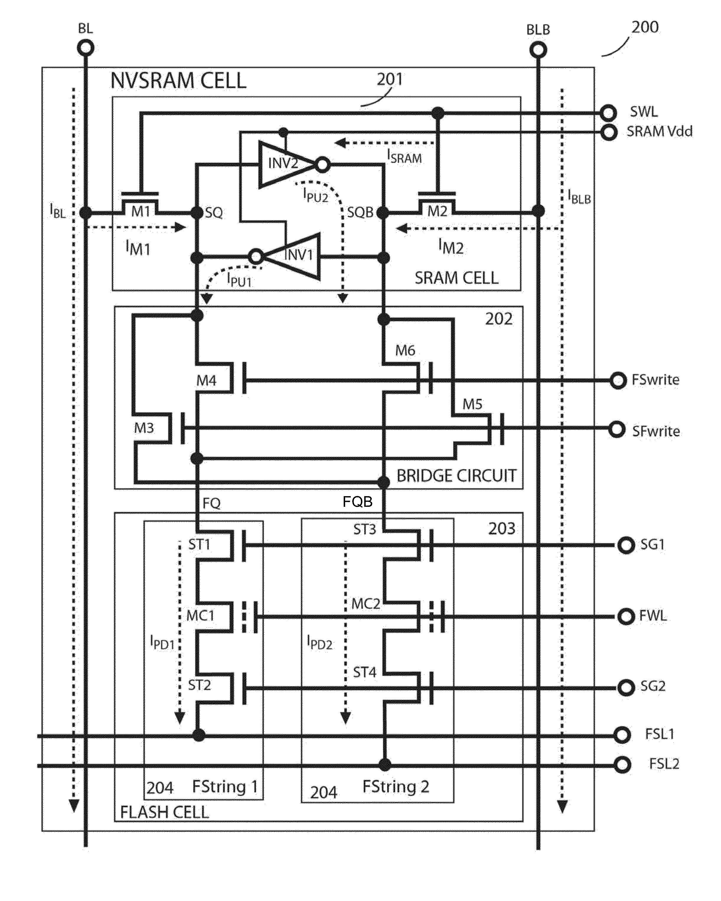
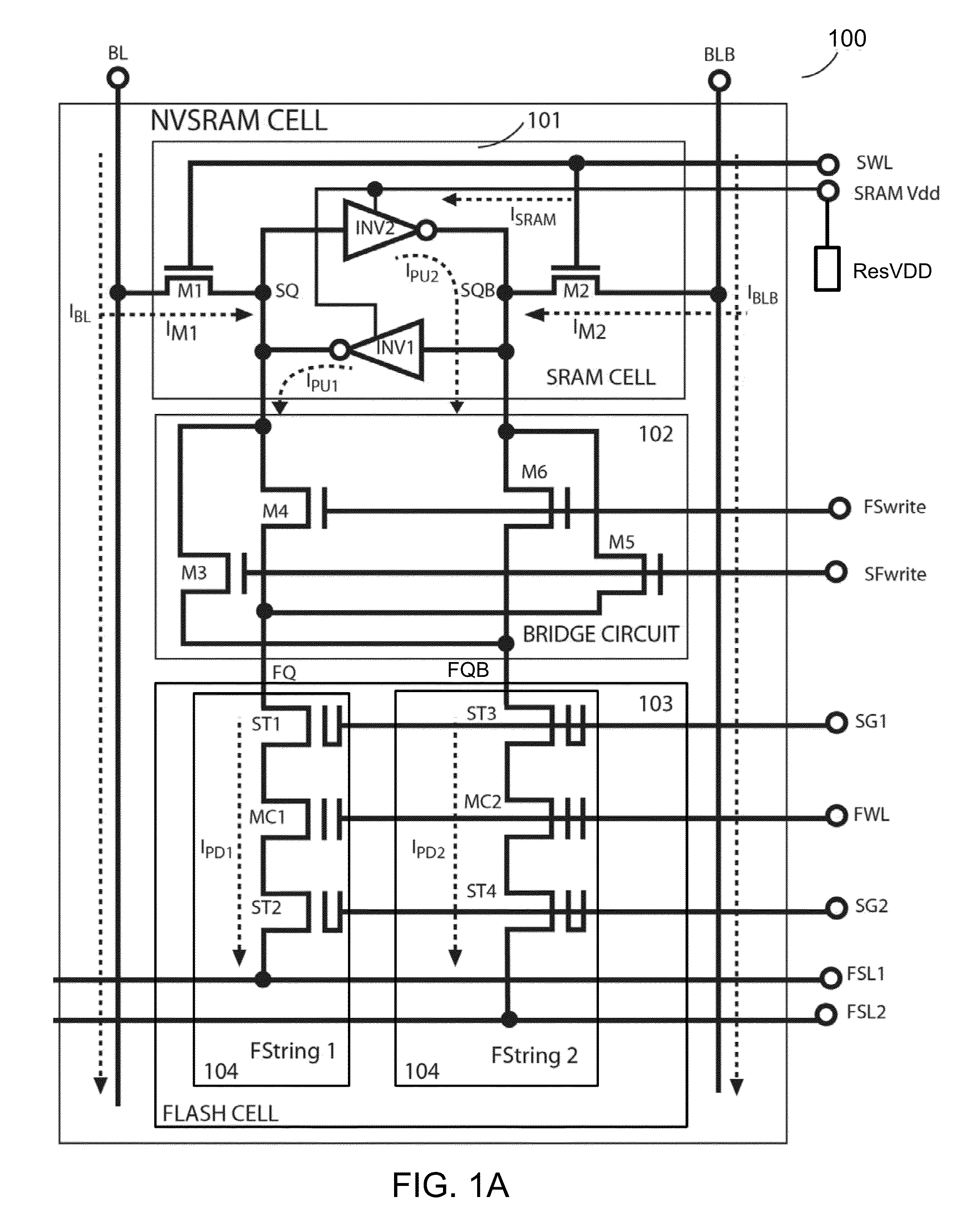
[0115] FSwrite for writing Flash Logic “0” state into SRAM.[0116]The operation of Case1 is illustrated with reference to DA1 explained above. There are two ways to write each Flash stored logic state into each SRAM. One way is to write each Flash cell logic data into each corresponding SRAM cell with the same polarity in Logic state by setting FSwrite=VDD and SFwrite=VSS. The other way is to write each Flash cell logic data into each corresponding SRAM cell with opposite polarity in Logic state by setting FSwrite=VSS and SFwrite=VDD. The FSwrite operation is under LV (low voltage VDD) operation. All related control signals of SG1, FWL, FSL1, FSL2 and SWL are all coupled to LV VDD.[0117]In application, FSwrite operation is performed upon a power-on period. For a LV operation like 1.2V VDD, this operation is preferably done after VDD stabilizes at 1.2V for more reliable operation. The SRAM data can be any logic state such as “0” or “1” before performing the FSwrite for this invention....

case2

[0121] FSwrite for writing Flash Logic “1” state into SRAM.[0122]Assume the paired Flash cells store the Logic “1” state, then MC1=Vt1 and MC2=Vt0 with the ΔVt=Vt1−Vt0. Under this “1” logic state along with a voltage of FWL higher than Vt0 and Vt1, then a current flow will happen on both FStrings with IPD1PD2 because VGS1 of MC1 is greater than VGS2 of MC2 where VGS1=VFWL−Vt0 and VGS2=VFWL−Vt1.[0123]But the current difference margin ΔI associated with IPD1PD2 can be secured for reliable setting by making resistor ResVDD a high-resistance as explained above. Thus the DA1 operation for the FSwrite for Logic “1” operation can be achieved reliably without a problem for LV operation even down to 1.2V VDD.

[0124]2) SFwrite operation:[0125]This operation is illustrated without reference to DA1, DA2 as explained above because for SFwrite operation, it does not involve any current flows between SRAM and Flash. It is the FN-tunneling effect happens to either MC1 or MC2 during SFwrite operation...


PUM


Abstract

Several preferred embodiments of 1S1F 16T NVSRAM, 1S1F 20T NVSRAM, 1S2F 22T NVSRAM, 1S2F 14T NVSRAM cells are proposed, regardless of 1-poly, 2-poly, PMOS or NOS flash cell structures. Two separate sourcelines for the paired flash Strings are also proposed for easy adding ability for the NVSRAM circuit to detect the marginally erased Vt0 and marginally programmed Vt1 of the paired flash cell. By increasing an resistance added to common SRAM power line, the pull-down current through flash Strings to grounding source line can be made much larger than the pull-up current to improve SFwrite program operation. Simple method by increasing flash cell channel length to effectively enhance coupling area is applied to secure SRAM-to-Flash store operation under self-boost-program-inhibit scheme. 1S2F architecture also provide flexibility for alternate erasing and programming during both a recall and store operation.

Description

CROSS-REFERENCES TO RELATED APPLICATIONS[0001]This application claims priority to U.S. Provisional Patent Application No. 61 / 705,597, filed on Sep. 25, 2012 and U.S. Provisional Patent Application No. 61 / 710,573, filed on Oct. 5, 2012, commonly assigned, and hereby incorporated by reference in its entirety herein for all purposes.[0002]Additionally, this application is related to U.S. Pat. Nos. 8,120,966, 8,120,959, 8,072,811, 7,688,612, 7,830,713, 8,233,320, 8,149,622, and U.S. patent applications Ser. No. 13 / 135,220, 13 / 199,785, 13 / 199,527, 13 / 888,134, 12 / 807,997, 61 / 275,148, 61 / 277,208, 61 / 574,632, and 61 / 687,227, commonly assigned, which are incorporated by reference herein for all purposes.[0003]Furthermore, this application is related to U.S. Pat. Nos. 5,065,362, 7,164,608, and 7,760,540.TECHNICAL FIELD OF THE INVENTION[0004]The present invention relates to several improved techniques and methods for operating the next-generation low-power Non-Volatile Static Random-Access Mem...

Claims


Application Information

Patent Timeline
IPC IPC(8): G11C14/00
CPCH01L21/0262G11C14/0063G11C15/046G11C16/0483H01L27/0207G11C11/005H10B10/12H10B69/00
Inventor LEE, PETER WUNG
Owner APLUS FLASH TECH
Why Eureka
Try Eureka