Differential temperature sensor and its capacitors in cmos/bicmos technology

a technology of capacitors and temperature sensors, applied in the field of temperature sensors, can solve the problems of affecting the switching speed of microelectronic devices, the execution speed of integrated circuit functions, and the mobility impairment of carriers, so as to avoid drawbacks and avoid the effect of affecting the detection and communication of

Inactive Publication Date: 2014-01-16
ST ERICSSON SA +1
View PDF6 Cites 9 Cited by
  • Summary
  • Abstract
  • Description
  • Claims
  • Application Information

AI Technical Summary

Benefits of technology

The patent describes a thermoelectric device that can detect temperature differences efficiently and without interfering with electrical disturbances. The device includes a substrate made of semiconducting material, an electrically insulating layer covering one surface of the substrate, and two thermocouples connected to the insulating layer. The insulating layer has two portions with different values of capacitance and thermal conductance. The device also includes first and second legs made of electrically conducting material, which are simultaneously formed and doped. The technical effects of the invention include efficient detection of temperature differences and improved accuracy of thermoelectric measurements.

Problems solved by technology

For example, the mobility of the carriers which depends greatly on the temperature can be impaired under these conditions.
An impairment of the mobility of the carriers proves detrimental for the switching speed of microelectronic devices in particular, and for the execution speed of the integrated circuit functions in general.
This type of temperature sensor is not very precise and consumes a permanent current which, although it is low, is very sensitive to the disturbances caused by capacitive coupling with the dense interconnections within the integrated circuits.
Furthermore, these sensors, made from silicon as the associated circuits, are also sensitive to the stray currents created by operation of the circuit.
In this context, this type of thermal sensor can be considered as not being suitable for dense integrated circuits with high frequencies of use.
This results in electric disturbances caused by capacitive couplings being able to impair transmission of the electric signal from the sensor to the management circuit.
Integration of the microelectronic circuit then becomes more complex and more costly.

Method used


Image

  • Differential temperature sensor and its capacitors in cmos/bicmos technology
  • Differential temperature sensor and its capacitors in cmos/bicmos technology
  • Differential temperature sensor and its capacitors in cmos/bicmos technology

Examples


Embodiment Construction

[0032]In order to benefit from the advantages of a management system of the dissipated power in an integrated circuit, it is preferable for this system to be associated with passive thermal sensors that are precise and easy to produce.

[0033]It is therefore advantageous to take advantage of Seebeck effect differential sensors produced by means of integrated circuit technology while at the same time avoiding electric disturbances which may occur on the output terminals of these sensors.

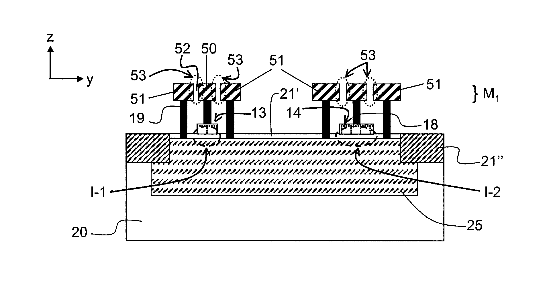
[0034]To overcome these drawbacks, it is envisaged to produce a differential thermal sensor that is electrically insulated from the substrate and provided with a capacitor connected in parallel with at least one of the two output terminals of the sensor, preferably with both of the output terminals of the sensor.

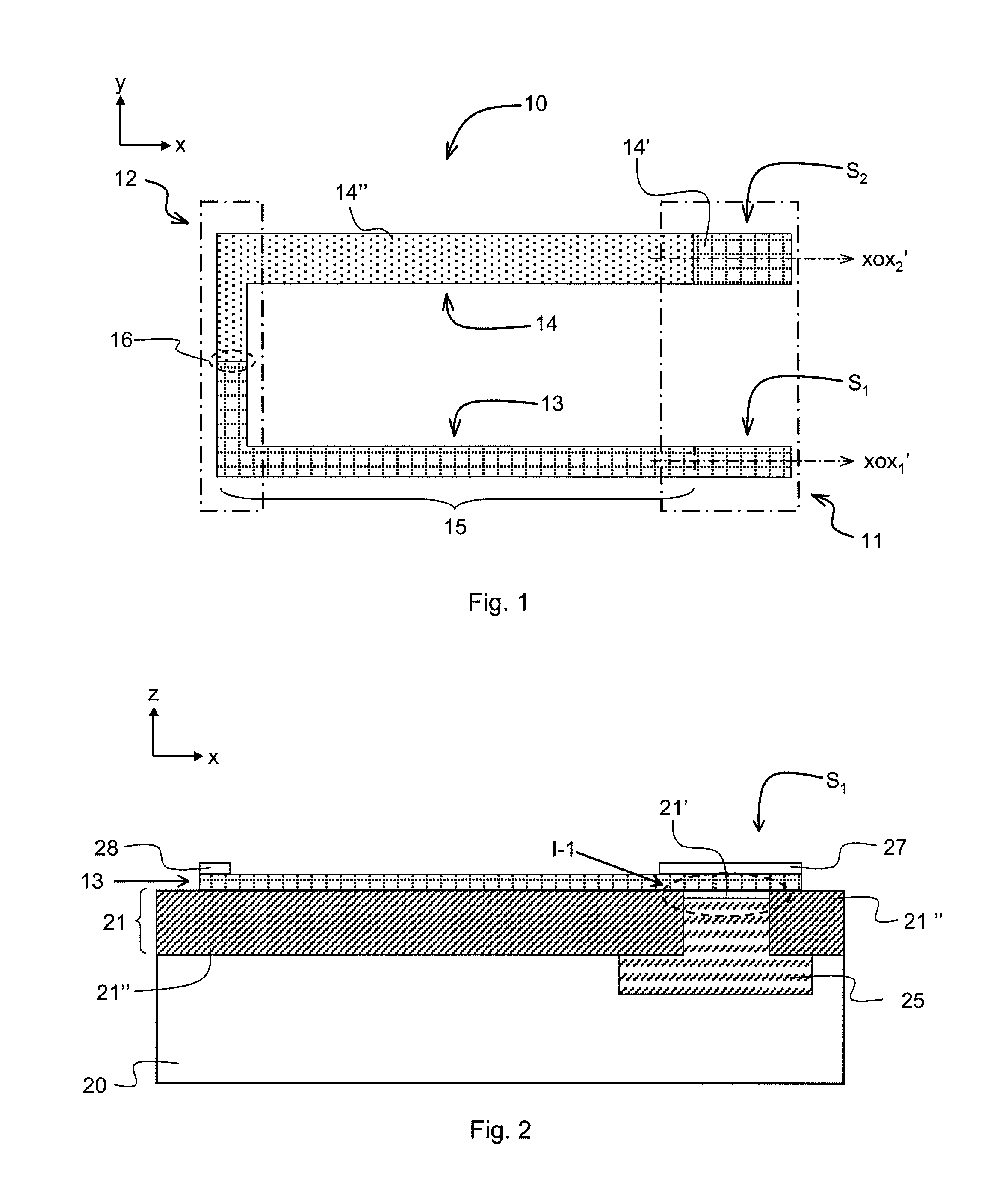
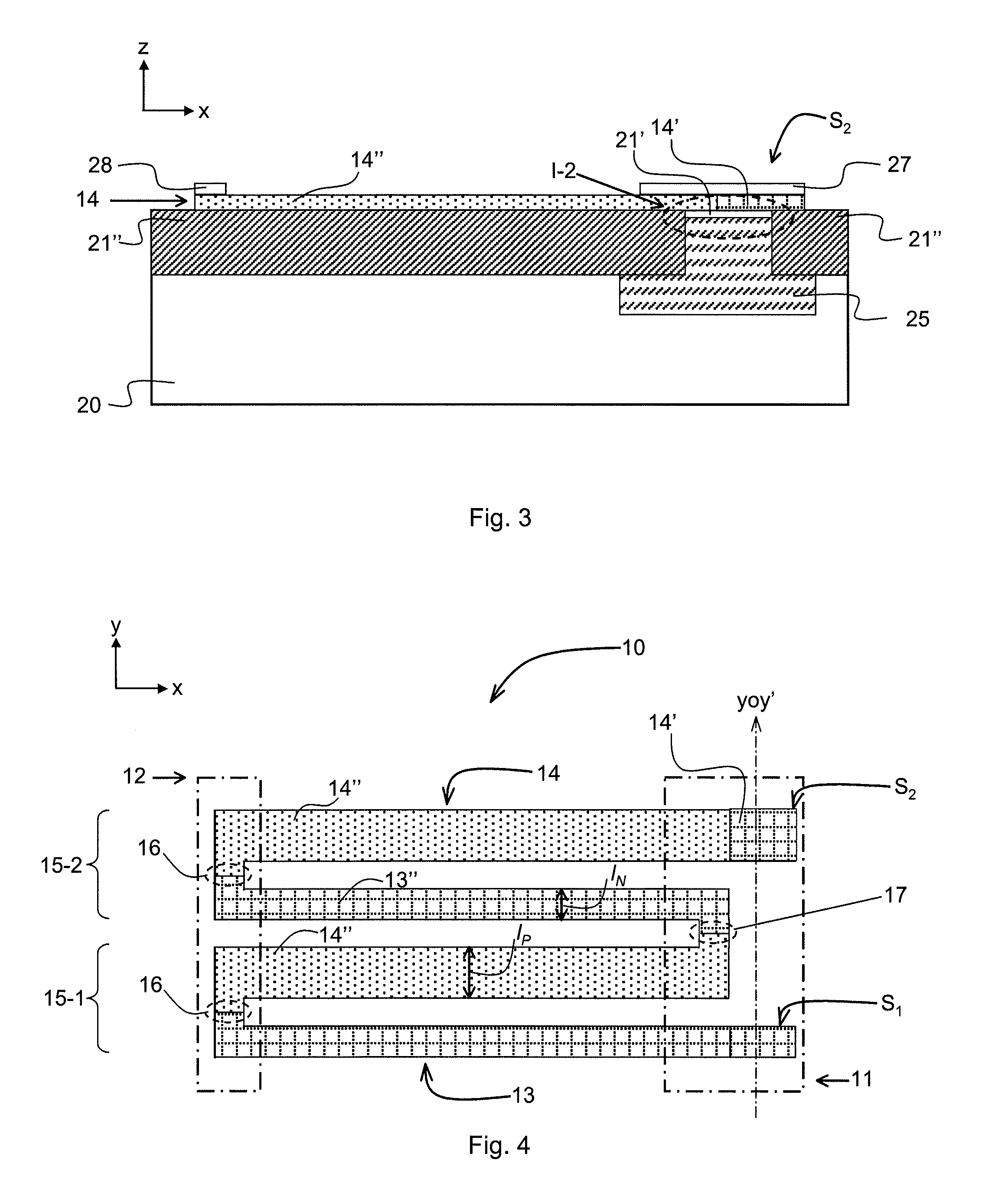
[0035]FIG. 1 schematically illustrates a top view of an embodiment of a thermo-electric device 10 which tends to meet these requirements. In operation, device 10 is arranged in a temperature gra...


PUM


Abstract

The sensor is made on a semiconductor substrate covered with an electrically insulating layer. The electrically insulating layer separates a thermocouple from the substrate. It includes a first portion presenting a first value of capacitance per unit area and a second portion presenting a second value of capacitance per unit area, which is lower than the first value. The sensor includes first and second output terminals connected to the thermocouple. The first output terminal includes a first capacitor having a first electrode formed by a first leg made of an electrically conducting material. The second electrode of the capacitor is formed by a part of the substrate facing said first leg and separated from the first electrode by the first portion of the electrically insulating layer. The first leg connects the thermocouple while overlapping the second portion of the electrically insulating layer.

Description

BACKGROUND OF THE INVENTION[0001]The invention relates to the field of temperature sensors, and more precisely to that of Seebeck effect differential sensors.[0002]The invention also relates to a method for co-integration of a Seebeck effect differential sensor and a field effect transistor.STATE OF THE ART[0003]With the increase of the integration density, the power dissipated in micro-electronic devices is continually increasing. The increase of the dissipated power can generate a phenomenon called self-heating, which is responsible for degradation of certain physical and electrical characteristics of the micro-electronic devices. For example, the mobility of the carriers which depends greatly on the temperature can be impaired under these conditions. An impairment of the mobility of the carriers proves detrimental for the switching speed of microelectronic devices in particular, and for the execution speed of the integrated circuit functions in general.[0004]At the present time, ...

Claims


Application Information

Patent Timeline
IPC IPC(8): G01K7/02H01L35/34
CPCG01K7/028H01L35/34H10N10/01
Inventor SAVELLI, GUILLAUMECOTTIN, DENIS
Owner ST ERICSSON SA
Why Eureka
Try Eureka