Method for Substrate Pretreatment To Achieve High-Quality III-Nitride Epitaxy

a technology of nitride and substrate, applied in the direction of polycrystalline material growth, chemistry apparatus and processes, crystal growth process, etc., can solve the problems of large majority of defects generated at the substrate-layer interface, epitaxial defects, and inability to meet the requirements of advanced device structures, such as laser diodes

Active Publication Date: 2013-12-19
OSTENDO TECH INC
View PDF0 Cites 230 Cited by
  • Summary
  • Abstract
  • Description
  • Claims
  • Application Information

AI Technical Summary

Benefits of technology

The present invention relates to a method for producing high-quality III-Nitride semiconductor substrates for the epitaxial growth of III-Nitrides semiconductor materials. The invention focuses on the second step in preparing the substrate for epitaxial growth, which is the fine tuning of the substrate surface to make it suitable for the material to be deposited. The invention is effective for both native and foreign substrates, which are important for the nitride semiconductor devices because of severe deficiencies in native substrates. The invention uses a combination of lapping, polishing, annealing, and degreasing to prepare the substrate surface for epitaxial growth. The invention is particularly useful for optoelectronic and power electronic devices that require exceptional quality epitaxial layers. Previous methods for preparing the substrate for epitaxial growth have resulted in high dislocation density, which negatively impacts the structural quality of the epilayers. The invention aims to improve the structural quality of the epilayers and achieve better uniformity in the distribution of dislocations.

Problems solved by technology

Reduction of the defects in the epitaxial III-Nitride layers has become a central issue in the development of the next generation III-Nitride devices.
Most notably, the vast majority of the defects are generated at the substrate-layer interface.
While some structural improvement of the epitaxial GaN is indeed observed, the dislocation density achieved by the disclosed method is still far above 108 cm−2 level, which is unacceptable for some advanced device structures, such as laser diodes, for example.
But difficulties to effectively control the uniformity and intensity of the treatment result in poor reproducibility of the process and non-uniform stress distribution in epitaxial layers.
Pretreatment with both ion beams results in the formation of a disordered amorphous phase on the substrate surface.

Method used


Image

  • Method for Substrate Pretreatment To Achieve High-Quality III-Nitride Epitaxy
  • Method for Substrate Pretreatment To Achieve High-Quality III-Nitride Epitaxy
  • Method for Substrate Pretreatment To Achieve High-Quality III-Nitride Epitaxy

Examples


embodiment 1

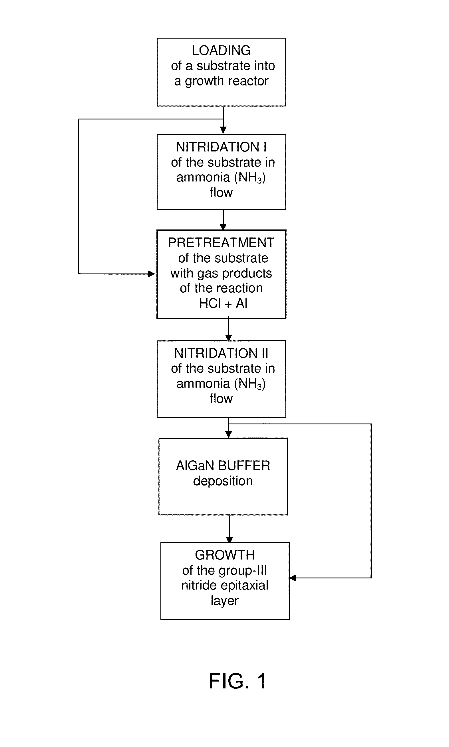
[0029]A (0001) sapphire (α-Al2O3) substrate is used for the pretreatment and subsequent epitaxial deposition of the gallium nitride (GaN) layer by hydride vapor-phase epitaxial (HVPE) technique. According to the present invention, pretreatment of the sapphire substrate is performed using gas-products of the reaction between aluminum (Al) and hydrogen chloride (HCl). The reaction takes place in the source zone of the reactor where metallic Al reacts with the gaseous HCl flowing over it. The transport of the gas products to the deposition zone is assisted by argon (Ar) as a carrier gas. However, carrier gases such as hydrogen (H), nitrogen (N), argon (Ar), helium (He) or their mixtures can also be used. Before and after the pretreatment, nitridation of the substrate in ammonia (NH3) gas flow and intermediary buffer layer deposition can be executed. The growth of GaN after the pretreatment employs gallium chloride (formed in the source zone of the reactor) and ultra-pure gaseous ammoni...

embodiment 2

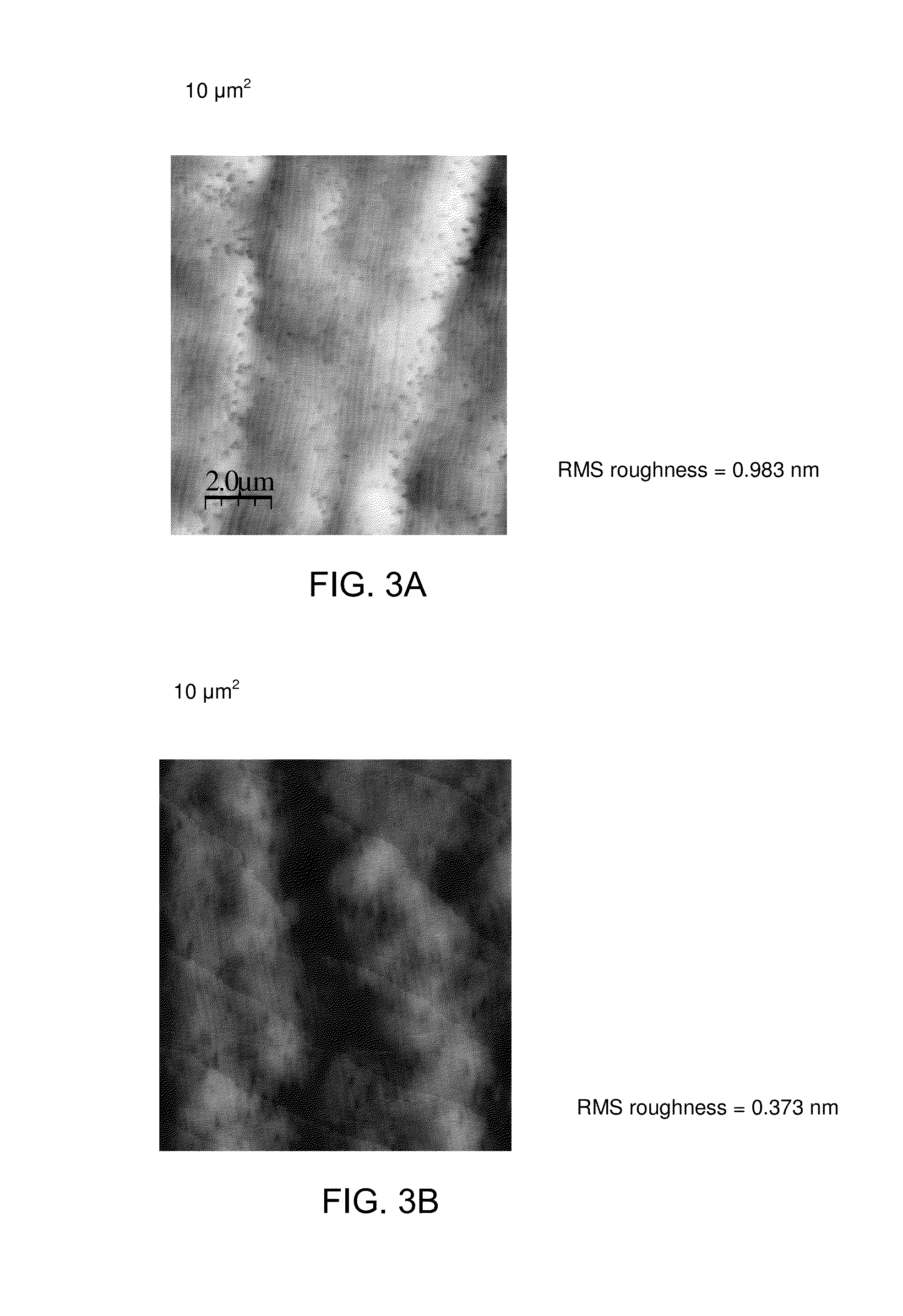
[0035]In another embodiment of the present invention, a (0001) 6H—SiC substrate is used as a substrate for the growth of AlN epilayer by the HVPE technique. The substrate is 3.5 degree off-oriented toward the a-plane. Again, according to the present invention, prior to the growth of the epilayer, the SiC substrate is subjected to the gas-products of the reaction between HCl and Al. After the pretreatment, deposition of AlN on Si-plane of the substrate is performed using aluminum chloride and ammonia as precursors for the group-III metal and nitrogen, respectively. Morphology and structural properties of the epilayer are analyzed by AFM and XRD, and compared to those of regular epilayers.

[0036]The pretreatment is carried out at 400 sccm HCl flow rate through the gas-channel containing high purity Al metal loading. The duration of the pretreatment is 14 min. After the pretreatment, the substrate is exposed to pure NH3 flow at 4 slm rate for 15 min to fulfill nitridation. Growth of the...


PUM


Abstract

The present invention relates to a method for producing a modified surface of a substrate that stimulates the growth of epitaxial layers of group-III nitride semiconductors with substantially improved structural perfection and surface flatness. The modification is conducted outside or inside a growth reactor by exposing the substrate to a gas-product of the reaction between hydrogen chloride (HCl) and aluminum metal (Al). As a single-step or an essential part of the multi-step pretreatment procedure, the modification gains in coherent coordination between the substrate and group-III nitride epitaxial structure to be deposited. Along with epilayer, total epitaxial structure may include buffer inter-layer to accomplish precise substrate-epilayer coordination. While this modification is a powerful tool to make high-quality group-III nitride epitaxial layers attainable even on foreign substrates having polar, semipolar and nonpolar orientation, it remains gentle enough to keep the surface of the epilayer extremely smooth. Various embodiments are disclosed.

Description

CROSS-REFERENCE TO RELATED APPLICATIONS[0001]This application claims the benefit of U.S. Provisional Patent Application No. 61 / 659,316 filed Jun. 13, 2012.BACKGROUND OF THE INVENTION[0002]1. Field of the Invention[0003]The present invention relates to III-V compound semiconductors and more particularly to a method for producing III-Nitride semiconductor substrate materials.[0004]2. Prior Art[0005]It would be considered common knowledge that for successful epitaxial growth, the proper preparation of a substrate surface is required. In general, the preparation consists of two major readily distinguishable steps. The first step is essentially similar for any substrate material and comprises lapping and polishing, annealing, degreasing and cleaning in organic and inorganic solvents. The second step is unique for every substrate material and can be regarded as a fine tuning of the substrate surface towards the material to be deposited. The present invention relates to the second step in ...

Claims


Application Information

Patent Timeline
IPC IPC(8): H01L21/205
CPCH01L21/0237H01L21/0242H01L21/02458H01L21/0254H01L21/02587H01L21/0262H01L21/02658C30B29/406C30B31/02
Inventor IVANTSOV, VLADIMIRVOLKOVA, ANNASHAPOVALOV, LISASYRKIN, ALEXANDERSPIBERG, PHILIPPEEL-GHOROURY, HUSSEIN S.
Owner OSTENDO TECH INC
Why Eureka
Try Eureka