Thin film transistor, manufacturing method therefor, and display device

a technology of thin film transistor and manufacturing method, which is applied in the direction of transistors, semiconductor devices, electrical devices, etc., can solve the problems of large current flow and increase the cost of production, and achieve the effect of reducing the off-current high resistance value, and fast operation speed of the thin film transistor

Active Publication Date: 2013-12-19
SHARP KK
View PDF4 Cites 23 Cited by
  • Summary
  • Abstract
  • Description
  • Claims
  • Application Information

AI Technical Summary

Benefits of technology

[0044]According to the first aspect, the second region having a higher resistance value than that in the first regions is extended not only to the channel region sandwiched between the source electrode and the drain electrode, but also to the end parts in the channel width direction of the channel layer. Accordingly, because the off-current flowing through the end parts in the channel width direction reduces, the off-current of the thin film transistor can be reduced.
[0045]According to the second aspect, because the source electrode and the drain electrode are overlapped with the gate electrode in the planar view, a high-concentration carrier layer is formed in the channel layer by the gate voltage applied to the gate electrode. Accordingly, the source electrode and the drain electrode become in ohmic contact with the channel layer.
[0046]According to the third aspect, because the source electrode and the drain electrode are not overlapped with the gate electrode in the planar view, a parasitic capacitance formed by the source electrode and the gate electrode and a parasitic capacitance formed by the drain electrode and the gate electrode become small. Accordingly, the operation speed of the thin film transistor can be made fast.
[0047]According to the fourth aspect, because the first regions of the channel layer are overlapped with the gate electrode in the planar view, the thin film transistor operates normally without becoming in the offset state.
[0048]According to the fifth aspect, one of the source electrode and the drain electrode is formed to be overlapped with the gate electrode in the planar view, and the other is formed not to be overlapped with the gate electrode. Accordingly, the parasitic capacitance of the thin film transistor can be set to approximately a half of the parasitic capacitance of the thin film transistor of which the source electrode and the drain electrode are overlapped with the gate electrode.
[0049]According to the sixth aspect, in the bottom gate type thin film transistor with the channel-etched structure, the off-current flowing through the end parts in the channel width direction reduces. Therefore, the off-current of the thin film transistor can be reduced.

Problems solved by technology

However, the TFT having an oxide semiconductor layer as a channel layer has a problem in that an off-current (the current flowing between a source electrode and a drain electrode in the off state) becomes large.

Method used


Image

  • Thin film transistor, manufacturing method therefor, and display device
  • Thin film transistor, manufacturing method therefor, and display device
  • Thin film transistor, manufacturing method therefor, and display device

Examples


first embodiment

1. First Embodiment

[0090]A liquid crystal display device according to a first embodiment of the present invention is described. The liquid crystal display device according to the present embodiment includes two kinds of TFTs. First, a configuration of each TFT is described.

[0091]

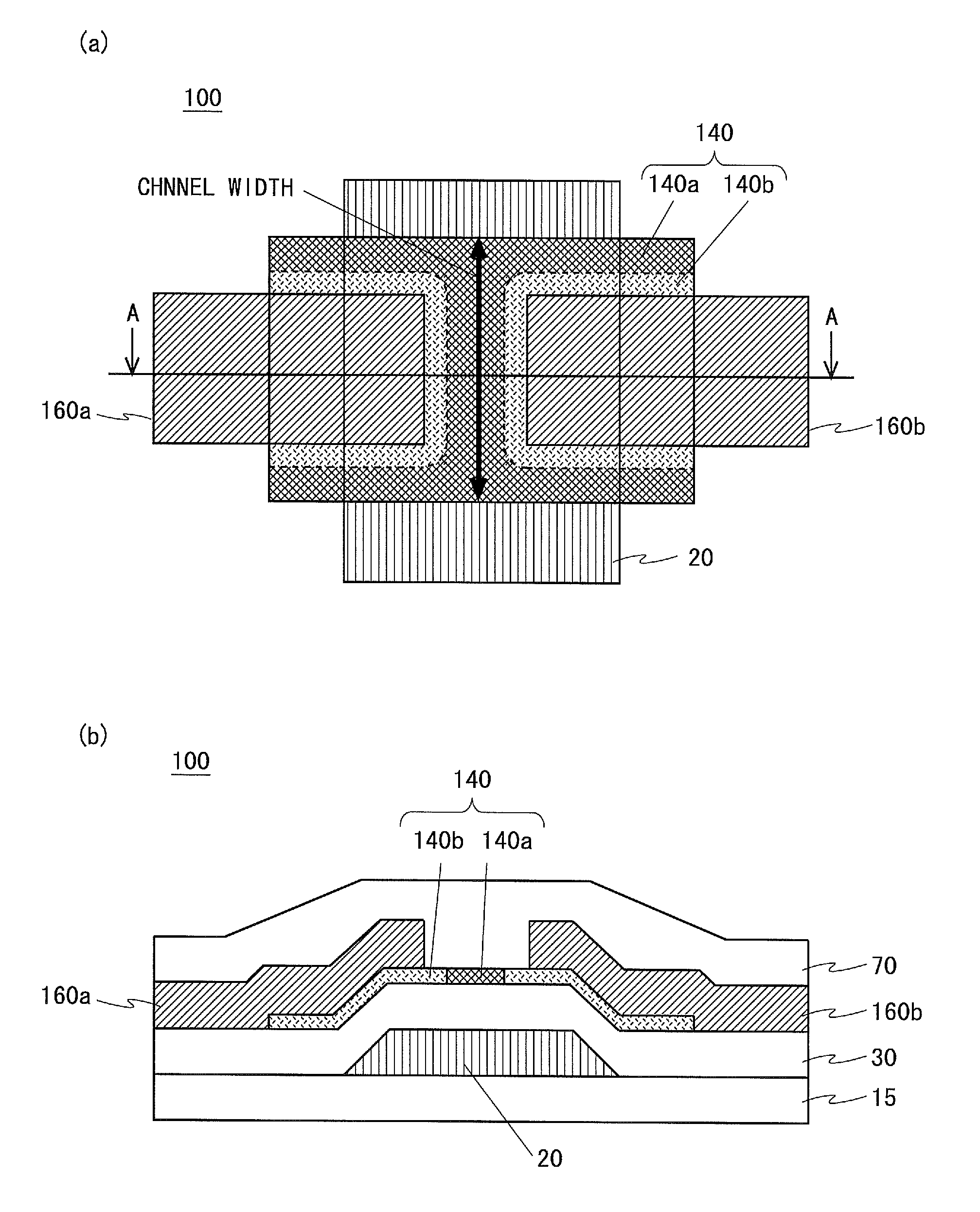
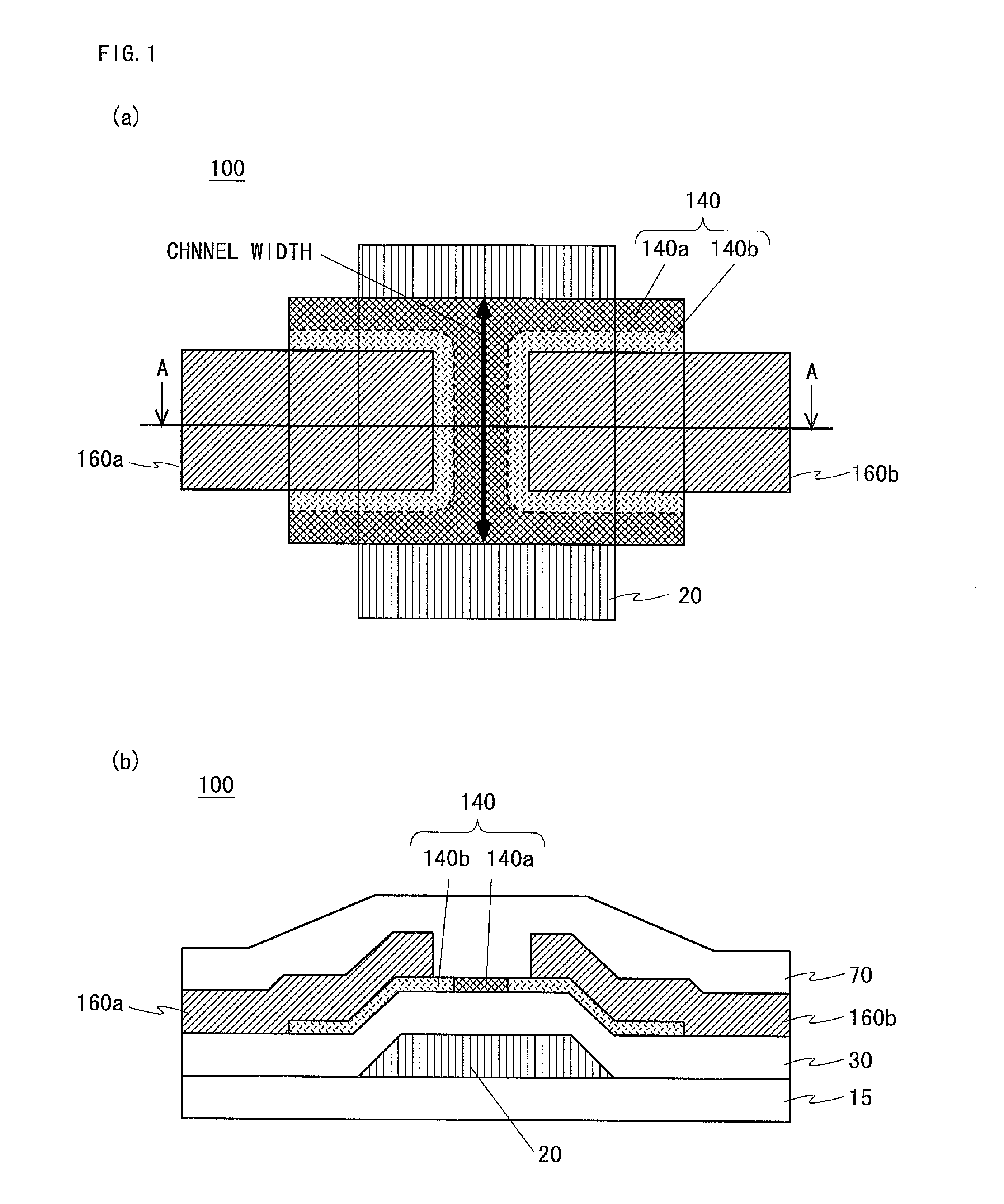
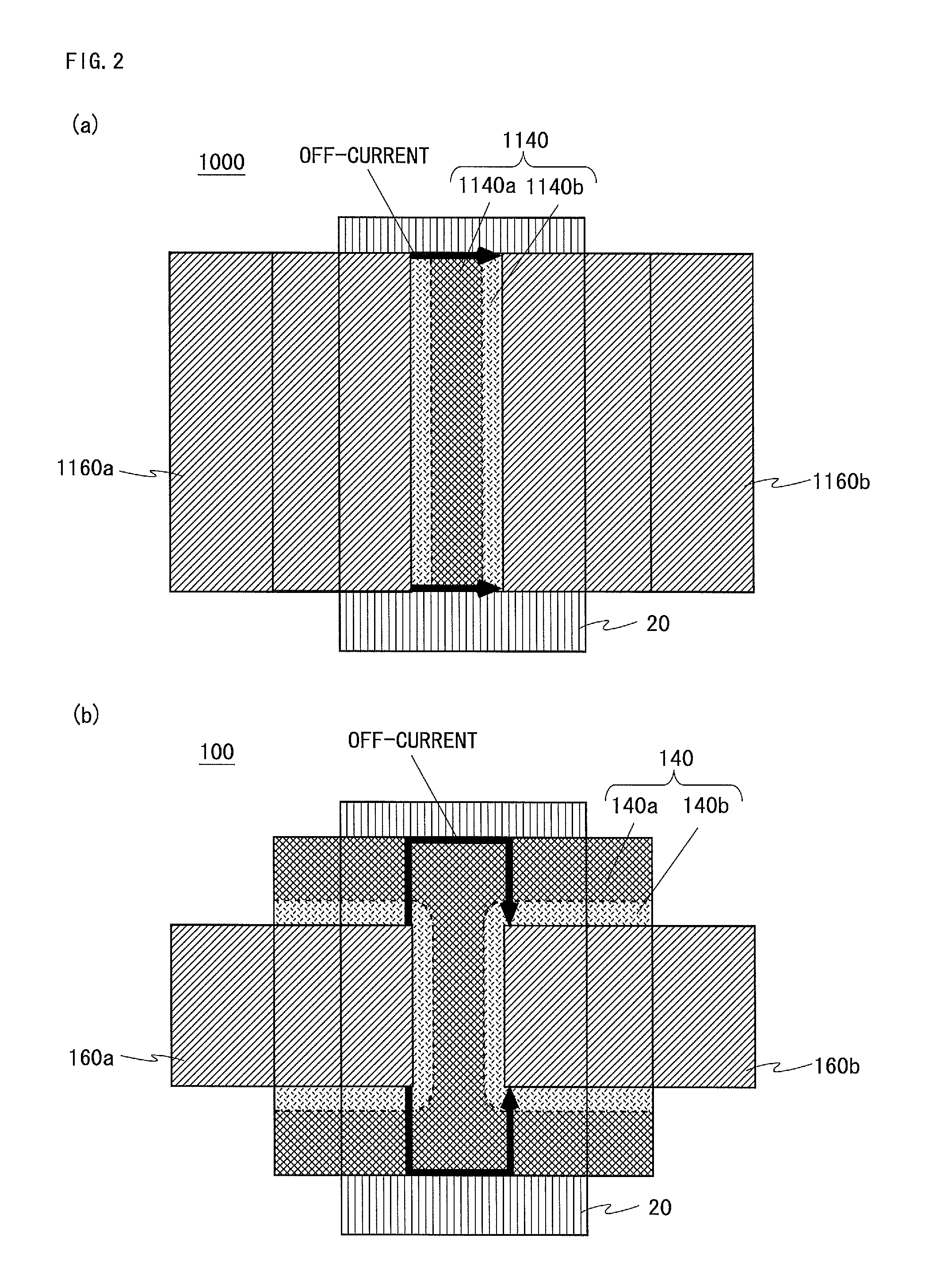
[0092]FIG. 1(a) is a plan view of a first bottom gate type TFT 100 included in a liquid crystal display device according to the present embodiment, and FIG. 1(b) is a cross-sectional view of the first bottom gate type TFT 100 taken along section line A-A shown in FIG. 1(a). The TFT 100 shown in FIG. 1(a) and FIG. 1(b) is also referred to as a TFT with a channel-etched structure. A configuration of the first bottom gate type TFT 100 is described with reference to FIG. 1(a) and FIG. 1(b). In the following description, the first bottom gate type TFT 100 is simply referred to as the TFT 100.

[0093]A gate electrode 20 is formed on an insulating substrate 15 such as a glass substrate. The gate electrode 20 is confi...

second embodiment

2. Second Embodiment

[0162]A liquid crystal display device according to a second embodiment of the present invention is described. The liquid crystal display device according to the present embodiment includes two kinds of TFTs. First, a configuration of each TFT is described.

[0163]

[0164]FIG. 13(a) is a plan view showing a configuration of a third bottom gate type TFT 300 included in the liquid crystal display device according to the present embodiment, and FIG. 13(b) is a cross-sectional view of the third bottom gate type TFT 300 taken along section line C-C shown in FIG. 13(a). The third bottom gate type TFT 300 shown in FIG. 13(a) and FIG. 13(b) is also referred to as a TFT with an etch stopper structure. A configuration of the third bottom gate type TFT 300 is described with reference to FIG. 13(a) and FIG. 13(b). In the following description, the third bottom gate type TFT 300 is referred to as the TFT 300. Out of components of the TFT 300, the components having the configuratio...

third embodiment

3. Third Embodiment

[0205]A liquid crystal display device according to a third embodiment of the present invention is described. The liquid crystal display device according to the present embodiment includes two kinds of TFTs. First, a configuration of each TFT is described.

[0206]

[0207]FIG. 19(a) is a plan view showing a configuration of a fifth bottom gate type TFT 500 included in the liquid crystal display device according to the present embodiment, and FIG. 19(b) is a cross-sectional view of the fifth bottom gate type TFT 500 taken along section line E-E shown in FIG. 19(a). The fifth bottom gate type TFT 500 shown in FIG. 19(a) and FIG. 19(b) are also referred to as a TFT with a bottom contact structure. A configuration of the fifth bottom gate type TFT 500 is described with reference to FIG. 19(a) and FIG. 19(b). In the following description, the fifth bottom gate type TFT 500 is referred to as the TFT 500. Out of components of the TFT 500, the components having the same configu...


PUM


Abstract

The invention provides a thin film transistor that can reduce an off-current flowing in end-parts in a channel width direction of a channel layer and a manufacturing method therefor.
Widths of a source electrode (160a) and a drain electrode (160b) are smaller than a width of a channel layer (140). Accordingly, in the channel layer (140), low resistance regions (140b) are formed to surround respectively the source electrode (160a) and the drain electrode (160b). A high resistance region (140a) having a higher resistance value than those of the low resistance regions (140b) remains not only in the region sandwiched between the two low resistance regions (140b), but also in the end parts in the channel width direction. As a result, in a TFT (100), the high resistance region (140a) is extended not only to the channel region sandwiched between the source electrode (160a) and the drain electrode (160b), but also to the end parts in the channel width direction. Accordingly, the off-current flowing through the end parts in the channel width direction reduces.

Description

TECHNICAL FIELD[0001]The present invention relates to a thin film transistor, a manufacturing method therefor, and a display device, and relates particularly to a thin film transistor having an oxide semiconductor layer as a channel layer, a manufacturing method therefor, and a display device.BACKGROUND ART[0002]A thin film transistor (hereinafter, referred to as a “TFT”) having an oxide semiconductor layer of indium gallium zinc oxide (hereinafter, referred to as “IGZO”) or the like as a channel layer has a characteristic in that the TFT has a fast operating speed as compared with a TFT having an amorphous silicon layer as a channel layer and that the TFT requires no crystallization process as compared with a TFT having a polycrystalline silicon layer as a channel layer. Therefore, in recent years, development of TFTs having an oxide semiconductor layer as a channel layer is being actively progressed.[0003]However, the TFT having an oxide semiconductor layer as a channel layer has ...

Claims


Application Information

Patent Timeline
Patent Type & Authority Applications(United States)
IPC IPC(8): H01L29/786H01L33/00
CPCH01L29/78693H01L33/0041H01L27/1222H01L29/41733H01L29/78609H01L29/78618H01L29/7869H01L29/78696
Inventor KATOH, SUMIOKITAKADO, HIDEHITO
Owner SHARP KK
Why Eureka
Try Eureka