Waveguide structure for mid-ir multiwavelength concatenated distributed-feedback laser with an active core made of cascaded stages
a distributed feedback and waveguide technology, applied in semiconductor lasers, optical radiation measurement, instruments, etc., can solve the problems of high power consumption and high loss of concatenated dfb qcls
- Summary
- Abstract
- Description
- Claims
- Application Information
AI Technical Summary
Benefits of technology
Problems solved by technology
Method used
Image
Examples
example 1
[0057]The waveguide structure in FIG. 6 was designed to demonstrate small far field angle, by guiding the light into the waveguide layers of GaInAs beneath the core layer, and expanding the optical mode. The short GaInAs layer (the first layer beneath the core) is located near the front facet, so that the light can only be guided into the waveguide layers near the front facet. The result was only partially successful. Light was guided into the waveguide structure as designed, as shown in FIG. 7, thus proving that we can guide light out at any chosen point, by placing the short first layer of GaInAs. However, due to the large width (for the purpose of small far field angle) of the waveguide layer, higher order modes were excited, instead of the fundamental mode. FIG. 8 shows that without the first layer of GaInAs, the light will not be guided into the 2nd waveguide layer as the overlap between the two optical modes is too small.
example 2
Prospective
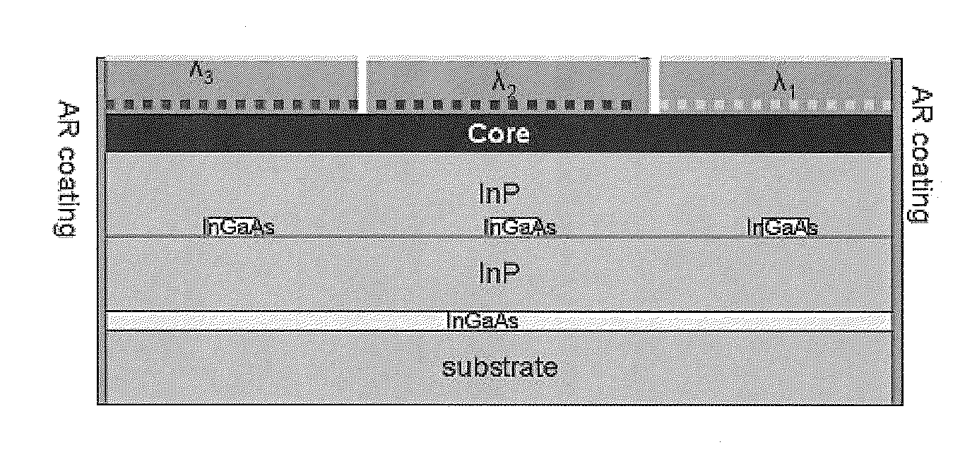
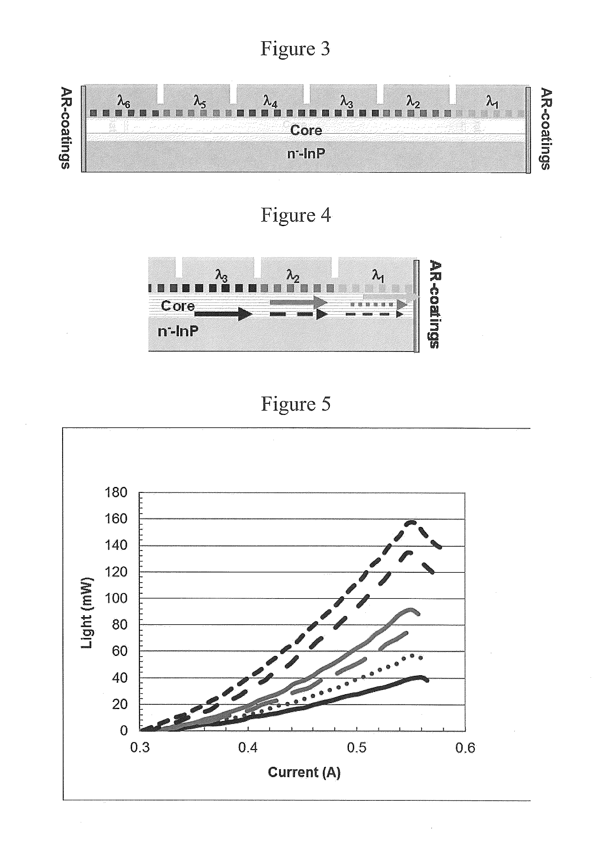
[0058]A proposed waveguide structure for the multiwavelength concatenated DFB QCL structure is shown in FIG. 9. The light emitted by each DFB section will be guided into the waveguide layer (e.g., GaInAs) beneath each section through the bridge layer (for example, comprising GaInAs). The bridge may be placed in the center of each DFB section, where the light intensity in a quarter-wave-shifted DFB structure reaches maximum. This structure comprises a single passive waveguide layer going through the whole structure and the design of this layer should be narrow enough (˜8 μm) to avoid higher order modes. Guiding the light through the passive waveguide will allow the light to experience much less loss because the loss of low-doped GaInAs is in the range of 1˜2 cm−1. It can be further reduced by reducing the doping in the GaInAs layers.
example 3
Prospective
[0059]An alternative proposed waveguide structure for the multiwavelength concatenated DFB QCL structure is shown in FIG. 11. FIG. 11A shows the top view of the structure wherein the bridge and passive waveguide are located to the side of the laser ridge. FIG. 11B describes the longitudinal cross section of the alternative waveguide, showing that the bridge is located at a height between the passive waveguide and the active layer. The waveguide layers may comprise any number of compositions that are transmissive at the requisite wavelength.
PUM
 Abstract
Description
Claims
Application Information
 - R&D
- Intellectual Property
- Life Sciences
- Materials
- Tech Scout
- Unparalleled Data Quality
- Higher Quality Content
- 60% Fewer Hallucinations
Browse by: Latest US Patents, China's latest patents, Technical Efficacy Thesaurus, Application Domain, Technology Topic, Popular Technical Reports.
© 2025 PatSnap. All rights reserved.Legal|Privacy policy|Modern Slavery Act Transparency Statement|Sitemap|About US| Contact US: help@patsnap.com


