Multiple distributed feedback laser devices
a laser device and distributed feedback technology, applied in the direction of lasers, lasers, semiconductor lasers, etc., can solve the problems of increasing manufacturing costs, complicated structure, and the apparatus of generating the thz wave using the photomixing method, and achieve the effect of superior reliability
- Summary
- Abstract
- Description
- Claims
- Application Information
AI Technical Summary
Benefits of technology
Problems solved by technology
Method used
Image
Examples
embodiment 1
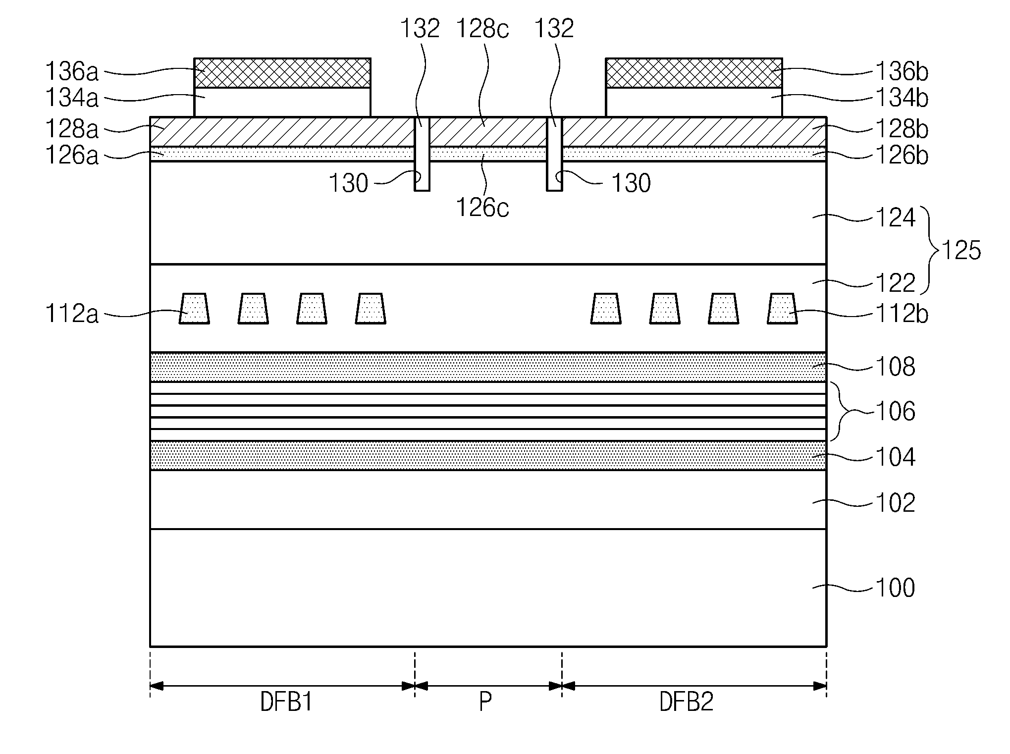
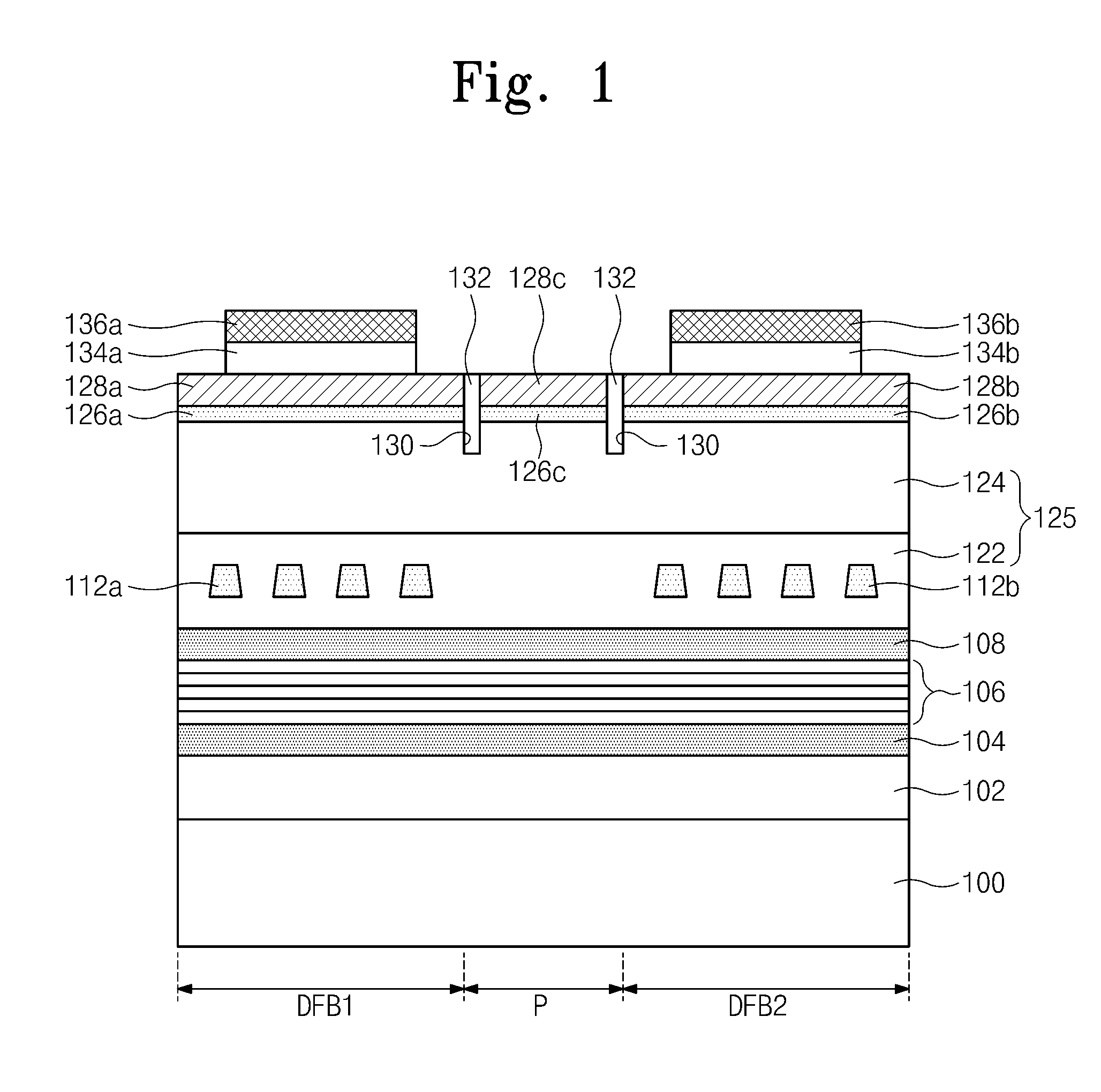
FIG. 1 is a cross-sectional view of a multiple distributed feedback laser device according to an embodiment of the present invention.
Referring to FIG. 1, a substrate 100 includes a first distributed feedback region DFB1, a modulation region P and a second distributed feedback region DFB2. An active layer 106 is disposed on the substrate 100. The active layer 106 is disposed in the first distributed feedback, modulation, and second distributed feedback regions DFB1, P, and DFB2 of the substrate 100. The modulation region P may be disposed between the first distributed feedback region DFB1 and the second distributed feedback region DFB2. The substrate 100 may be formed of a compound semiconductor. For example, the substrate 100 may include an indium-phosphorus (InP) substrate.
The active layer 106 may be continuously disposed along the first distributed feedback, modulation, and second distributed feedback regions DFB1, P, and DFB2 of the substrate 100. The active layer 106 may be form...
embodiment 2
FIG. 3A is a top plan view of a multiple distributed feedback laser device according to another embodiment of the present invention, and FIG. 3B is a cross-sectional view taken along the line I-I′ in FIG. 3A.
Referring to FIGS. 3A and 3B, a substrate 200 includes a first distributed feedback region DFB1, a modulation region P, a second distributed feedback region DFB2, and an amplification region AMP. The modulation region P may be disposed between the first distributed feedback region DFB1 and the second distributed feedback region DFB2. The amplification region AMP may be disposed at one side of the second distributed feedback region DFB2. That is, the second distributed feedback region DFB2 may be disposed between the modulation region P and the amplification region AMP.
An active layer 106 is disposed on the substrate 200. The active layer 206 is preferably disposed in the first distributed feedback, modulation, and second distributed feedback regions DFB1, P, and DFB2 of the subs...
embodiment 3
A multiple distributed feedback laser device according to this embodiment is similar to that described with reference to FIGS. 3A and 3B. The same numerals in this embodiment as those in the first embodiment denote the same elements.
FIG. 6A is a top plan view of a multiple distributed feedback laser device according to yet another embodiment of the present invention, FIG. 6B is a cross-sectional view taken along the line II-II′ in FIG. 6A, and FIG. 6C is a cross-sectional view taken along the line III-III′ in FIG. 6A. FIG. 7 is a cross-sectional view illustrating a modified embodiment of the multiple distributed feedback laser device according to yet another embodiment of the present invention.
Referring to FIGS. 6A, 6B, and 6C, an isolation trench 230 may be formed at an upper portion of an upper cladding layer 225 and filled with an isolation dielectric pattern 232. The isolation trench 230 may divide the upper cladding layer 225 into a first region, a second region, a third region...
PUM
 Abstract
Description
Claims
Application Information
 - R&D
- Intellectual Property
- Life Sciences
- Materials
- Tech Scout
- Unparalleled Data Quality
- Higher Quality Content
- 60% Fewer Hallucinations
Browse by: Latest US Patents, China's latest patents, Technical Efficacy Thesaurus, Application Domain, Technology Topic, Popular Technical Reports.
© 2025 PatSnap. All rights reserved.Legal|Privacy policy|Modern Slavery Act Transparency Statement|Sitemap|About US| Contact US: help@patsnap.com


