Photomask and semiconductor apparatus manufacturing method
a manufacturing method and semiconductor technology, applied in the direction of microlithography exposure apparatus, photomechanical treatment, instruments, etc., can solve the problem of difficult densely arranged pattern
- Summary
- Abstract
- Description
- Claims
- Application Information
AI Technical Summary
Benefits of technology
Problems solved by technology
Method used
Image
Examples
first embodiment
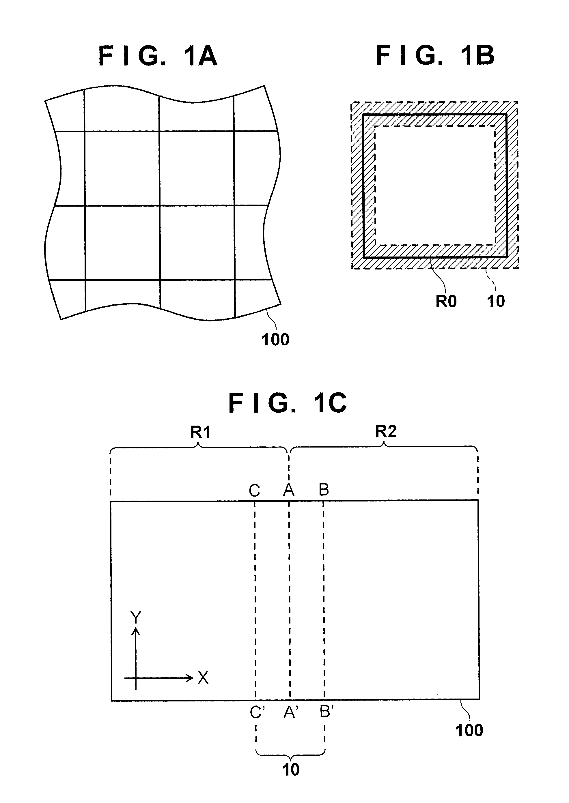
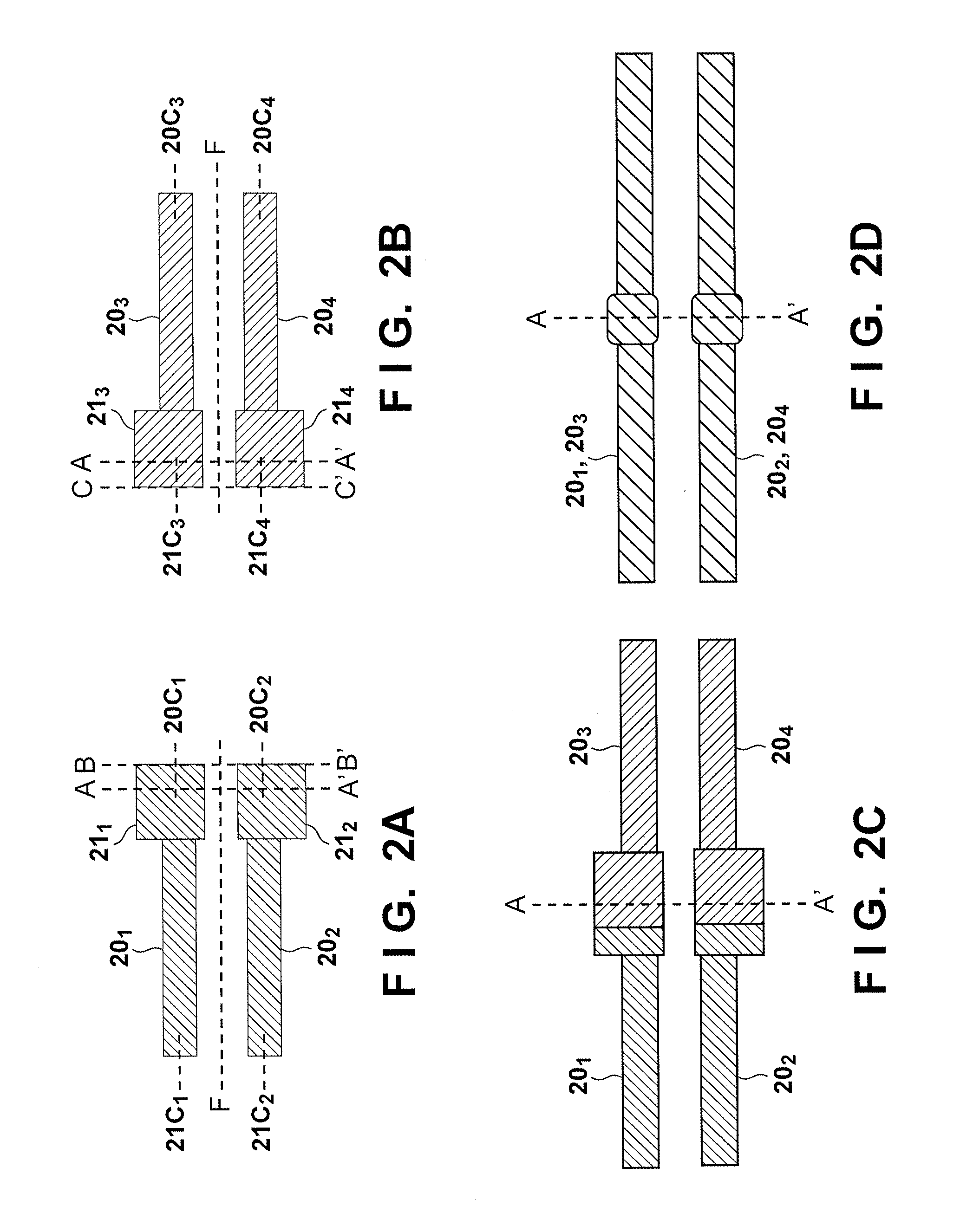
[0014]A photomask and a semiconductor apparatus manufacturing method (especially an exposure method) according to the first embodiment will be described with reference to FIGS. 1A to 3B. As illustrated in FIG. 1A, when a region in which a device or chip is to be formed on a substrate 100 is divided into a plurality of regions, and the plurality of regions are exposed individually, a portion (to be referred to as a “peripheral portion” hereinafter) which reflects an alignment error of a photomask is formed on the periphery of each region. FIG. 1B shows one region R0 of the plurality of regions, and its peripheral portion 10. The peripheral portion 10 includes inner and outer parts of the region R0. That is, the mask pattern of each photomask used in a corresponding exposure process includes the pattern of a region in which a device or chip is to be formed, and the pattern of the peripheral portion of the region. Line patterns to extend across the region R0 and adjacent regions, for e...
second embodiment
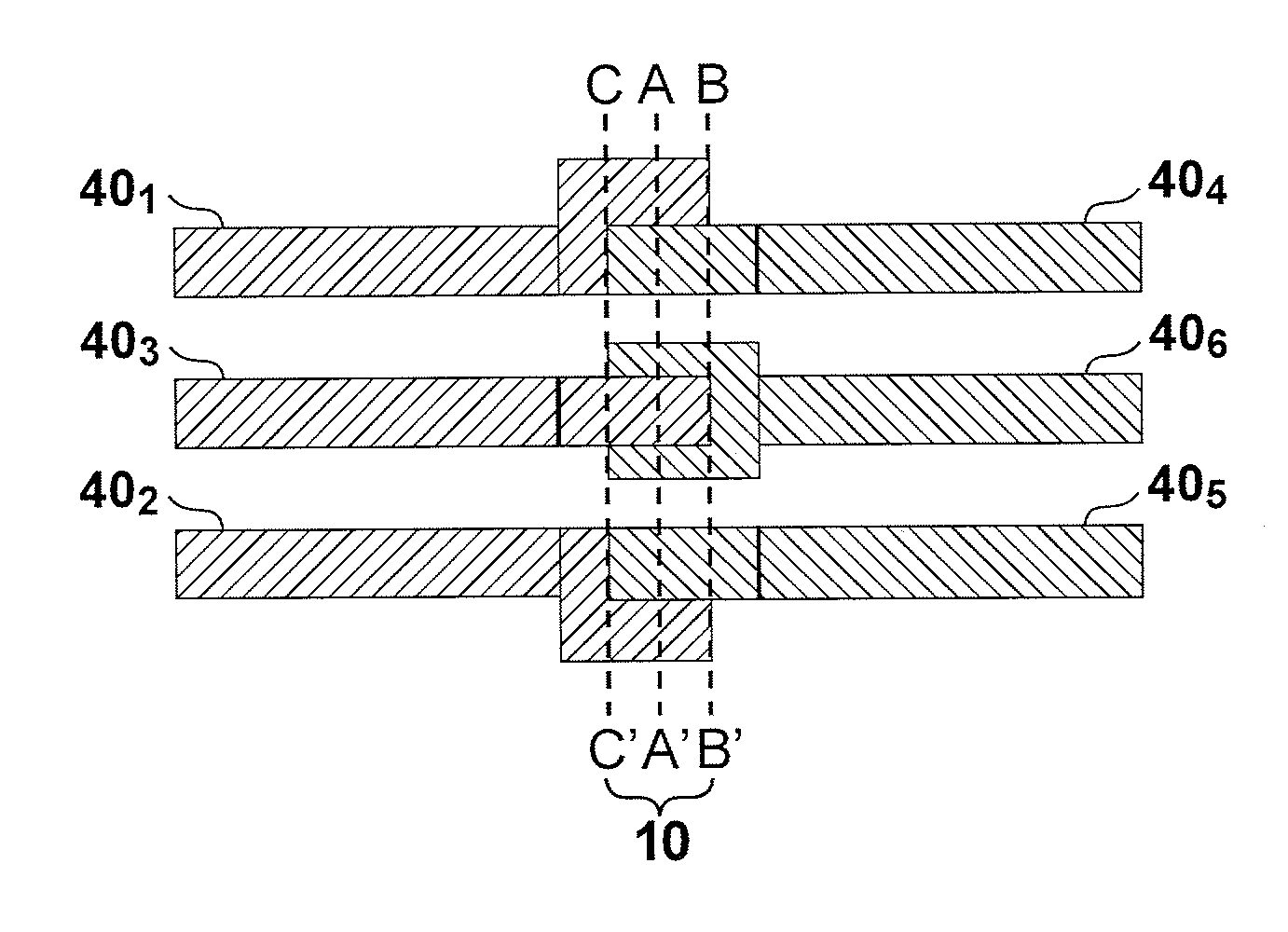
[0022]A photomask and a semiconductor apparatus manufacturing method (especially an exposure method) according to the second embodiment will be described with reference to FIGS. 4A to 4D. As in the first embodiment, the case wherein a semiconductor integrated circuit pattern is formed by individually exposing two adjacent regions (a first region R1 and a second region R2) on a substrate will be considered below.
[0023]First, a first region R1 and its peripheral portion 10 on a substrate 100 coated with, for example, a positive photoresist material are exposed using a photomask for forming a pattern as illustrated in FIG. 4A (first step). The mask pattern of the photomask used in the first step includes first to third line patterns 401 to 403 and first to third connection patterns 411 to 413. Each of the first line pattern 401 and second line pattern 402 is arranged in the first region R1 along a first direction X. The third line pattern 403 is arranged in the first region R1 along th...
third embodiment
[0028]The third embodiment will be described with reference to FIGS. 5A to 5D. The third embodiment is different from the second embodiment in the following points. First, the distance from a virtual line F1 to a center line 41C1 of a first connection pattern 411 is larger than that from the virtual line F1 to a center line 40C1 of a first line pattern 401, as shown in FIG. 5A. Note that the virtual line F1 runs in a first direction X between the first line pattern 401 and a third line pattern 403. Also, the distance from a virtual line F2 to a center line 41C2 of a second connection pattern 412 is larger than that from the virtual line F2 to a center line 40C2 of a second line pattern 402, as shown in FIG. 5B. Note that the virtual line F2 runs in the first direction X between the second line pattern 402 and the third line pattern 403. The virtual line F1 and the Virtual line F2 extend along the first direction X.
[0029]For example, the first to third connection patterns 411 to 413 ...
PUM
 Abstract
Description
Claims
Application Information
 - R&D
- Intellectual Property
- Life Sciences
- Materials
- Tech Scout
- Unparalleled Data Quality
- Higher Quality Content
- 60% Fewer Hallucinations
Browse by: Latest US Patents, China's latest patents, Technical Efficacy Thesaurus, Application Domain, Technology Topic, Popular Technical Reports.
© 2025 PatSnap. All rights reserved.Legal|Privacy policy|Modern Slavery Act Transparency Statement|Sitemap|About US| Contact US: help@patsnap.com


