Transparent conductive film and manufacturing method therefor
a technology manufacturing method, which is applied in the direction of cable/conductor manufacturing, vacuum evaporation coating, coating, etc., can solve the problems of poor transparency film has strong yellow tint, and cannot be sputtered at high temperature, etc., to achieve short time, improve the productivity of transparent conductive film, and low resistance
- Summary
- Abstract
- Description
- Claims
- Application Information
AI Technical Summary
Benefits of technology
Problems solved by technology
Method used
Image
Examples
example 1
Formation of the Anchor Layer
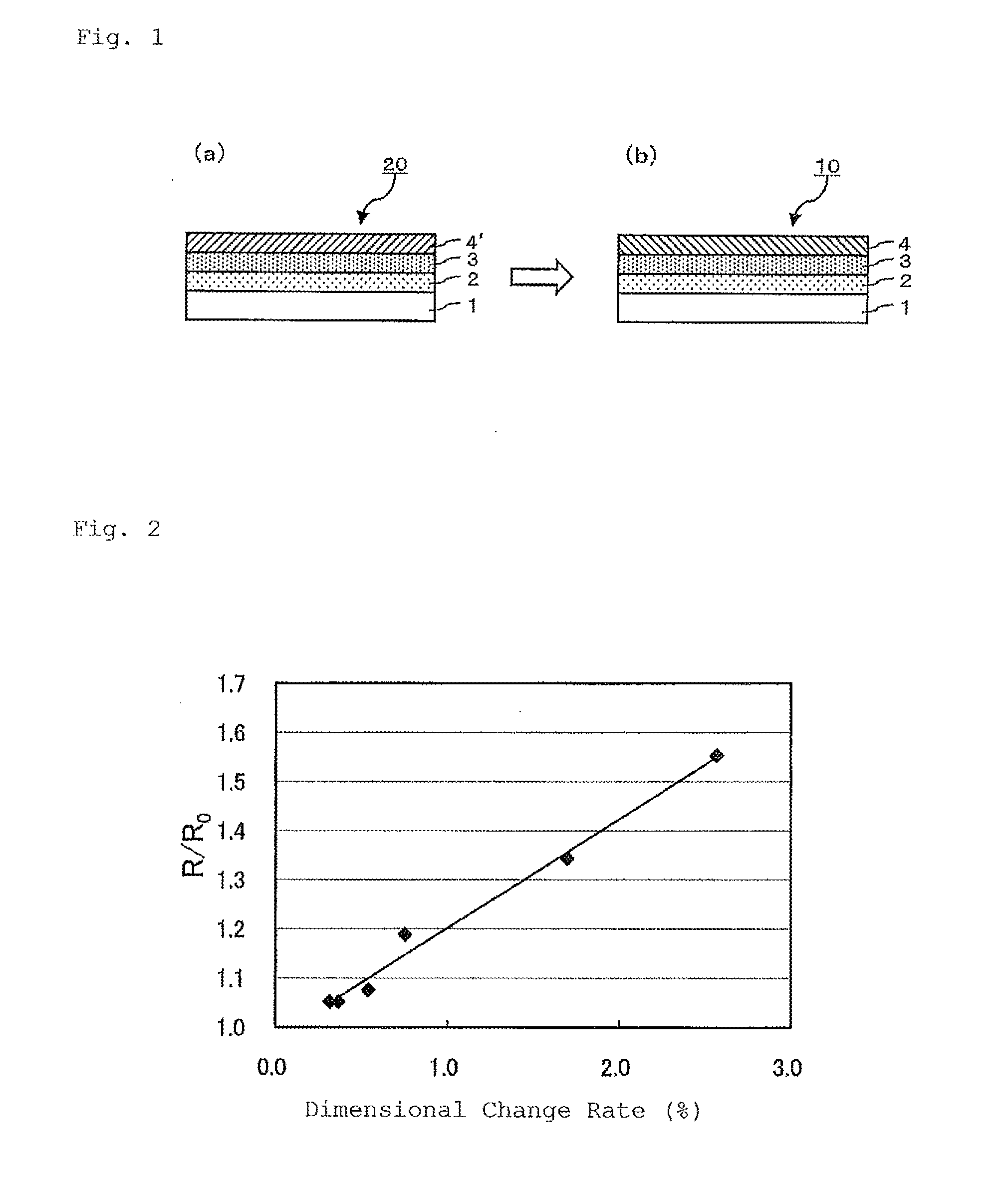
[0086]Two undercoat layers were formed on a biaxially oriented polyethylene terephthalate film (trade name “Diafoil” manufactured by Mitsubishi Plastics, Inc., glass transition temperature 80° C., refractive index 1.66) having a thickness of 23 μm with a roll-to-roll method. A thermosetting resin composition containing a melamine resin, an alkyd resin, and an organic silane condensate at a weight ratio of 2:2:1 in solid content was diluted with methylethylketone so that the concentration of the solid content was 8% by weight. This solution was applied on one of the main surfaces of a PET film, and it was heated and cured at 150° C. for 2 minutes to form a first undercoat layer having a thickness of 150 nm and a refractive index of 1.54.
[0087]A siloxane thermosetting resin (“Colcoat P” manufactured by COLCOAT CO., LTD.) was diluted with methylethylketone so that the concentration of solid content was 1% by weight. This solution was applied onto the first ...
example 2
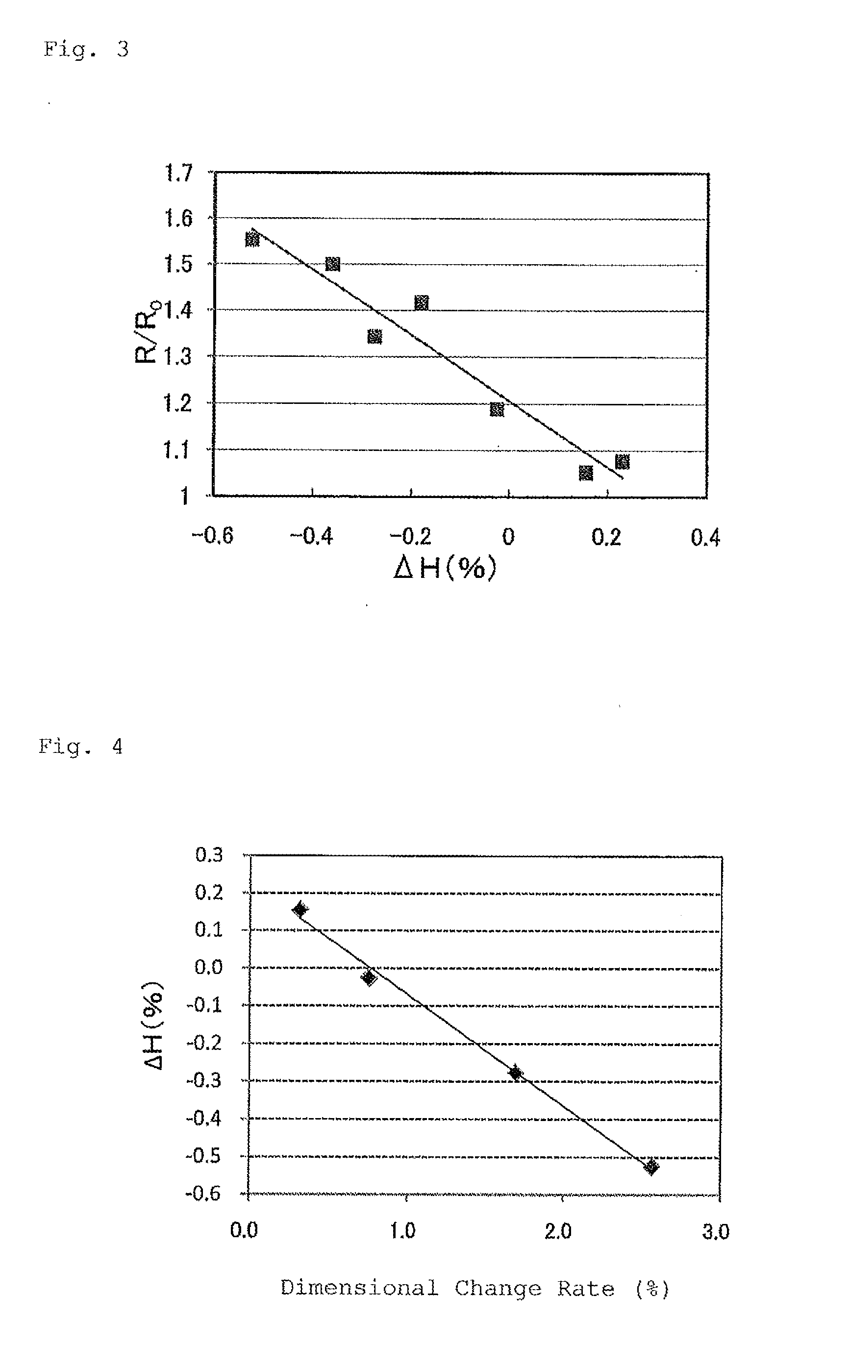
[0091]In Example 2, a roll of a transparent conductive film on which a crystalline ITO film was formed was formed in the same manner as in Example 1. However, it was different from Example 1 only in a respect that the feeding tension per unit width of the film in the furnace in the crystallization step was set to 51 N / m.
example 3
[0092]In Example 3, a roll of a transparent conductive film on which a crystalline ITO film was formed was formed in the same manner as in Example 1. However, it was different from Example 1 only in a respect that the feeding tension per unit width of the film in the furnace in the crystallization step was set to 65 N / m.
PUM
| Property | Measurement | Unit |
|---|---|---|
| temperature | aaaaa | aaaaa |
| temperature | aaaaa | aaaaa |
| thickness | aaaaa | aaaaa |
Abstract
Description
Claims
Application Information
 - R&D
- Intellectual Property
- Life Sciences
- Materials
- Tech Scout
- Unparalleled Data Quality
- Higher Quality Content
- 60% Fewer Hallucinations
Browse by: Latest US Patents, China's latest patents, Technical Efficacy Thesaurus, Application Domain, Technology Topic, Popular Technical Reports.
© 2025 PatSnap. All rights reserved.Legal|Privacy policy|Modern Slavery Act Transparency Statement|Sitemap|About US| Contact US: help@patsnap.com


