
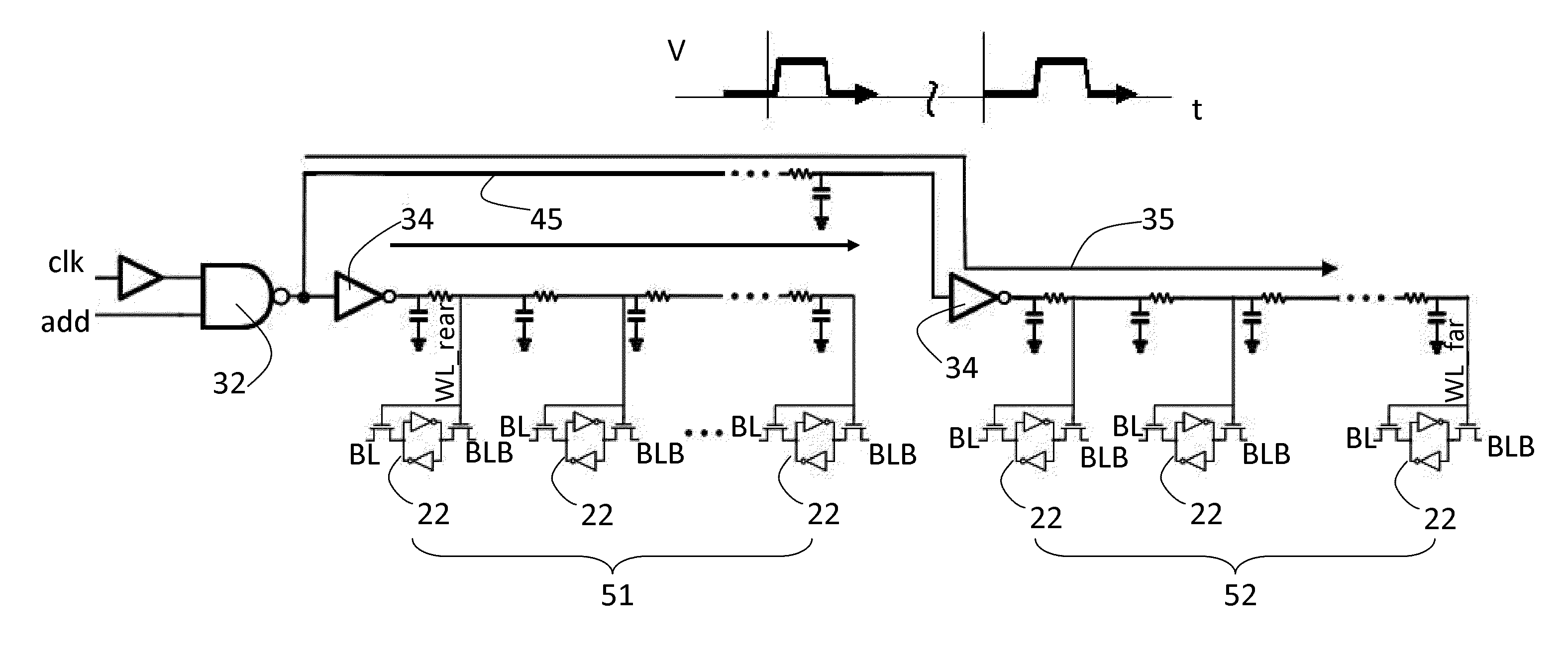
Fly-over conductor segments in integrated circuits with successive load devices along a signal path

a technology of integrated circuits and conductor segments, which is applied in the direction of time-delay networks, instruments, multiple-port active networks, etc., can solve the problems of poor slew rate on the rising and falling edges of pulses at the farthest bit cells, insufficient single-line driver or gate output to drive all load devices, and insufficient maximum operational frequency of circuits containing such load devices. , to achieve the effect of minimizing propagation delay and greater resistan

Active Publication Date: 2013-02-28
TAIWAN SEMICON MFG CO LTD
View PDF6 Cites 6 Cited by
  • Summary
  • Abstract
  • Description
  • Claims
  • Application Information

AI Technical Summary

Benefits of technology

The disclosed embodiments aim to make it easier for digital devices to operate when multiple loads are connected along a signal conductor. This is done by subdividing the conductor into multiple sections, each with its own driver, to ensure sufficient voltage swing and high slew rate at the loads that are farthest from the signal source. This solution also reduces propagation delay and improves pulse rise times, making it suitable for scalable layouts and production processes.

Problems solved by technology

Any or all of these conditions can be such that a single line driver or gate output is not sufficient to drive all of the loads.
The maximum operational frequency of circuits containing such load devices may be limited by the delay needed to establish necessary levels and to apply necessary clocking edges, dependably, at the remotest and / or slowest of the switched circuit elements.
A situation may occur in which the word line is sufficiently long that the slew rate on the rising and falling edges of the pulse at the farthest bit cell is poor.
Or the pulse may not achieve a full swing between respective logic states at the farthest bit.
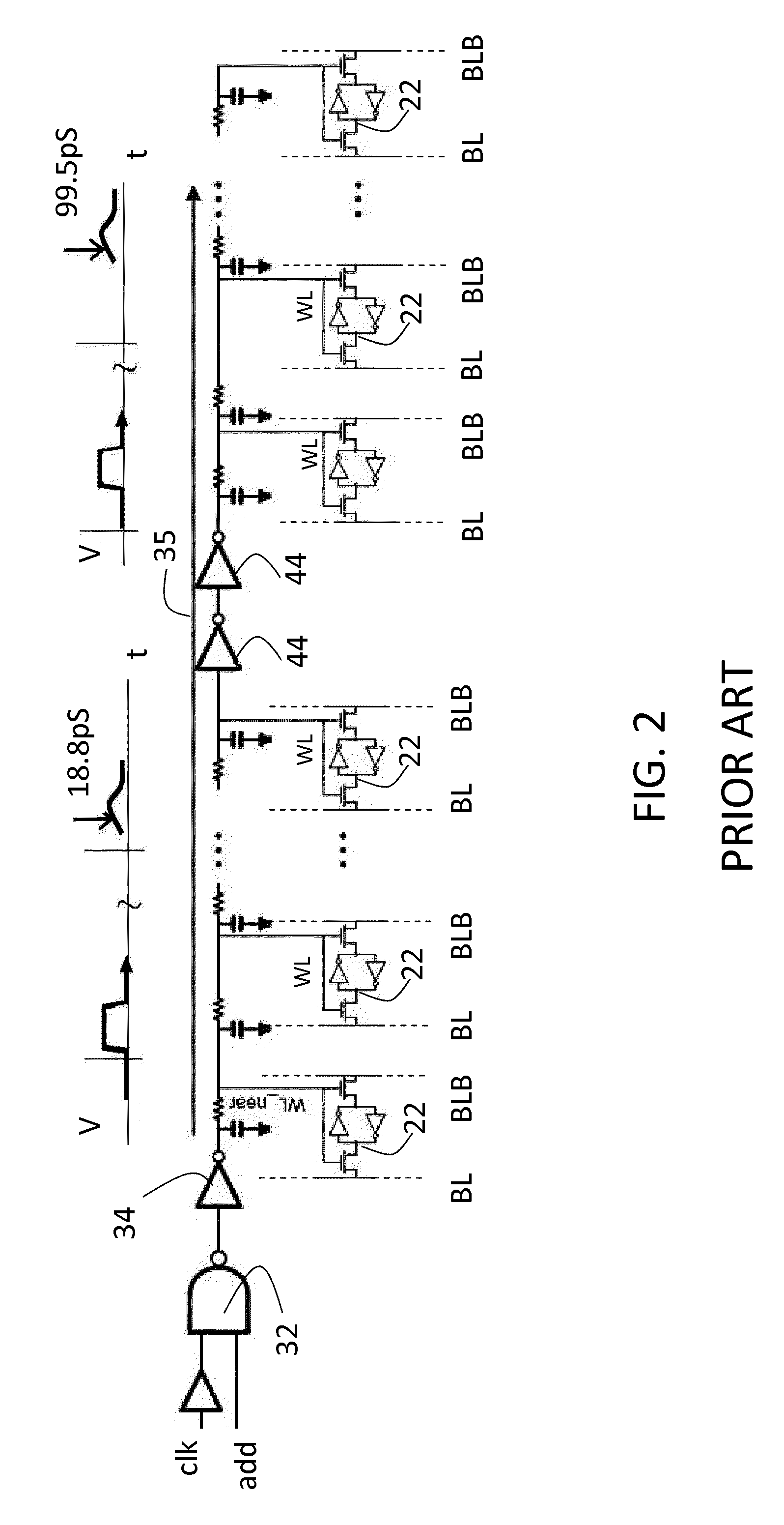
The repeater drives the signal to the more distant elements, but each inverter adds an additional propagation delay.
However, the line driver inserts a propagation delay even in addition to the propagation delay resulting from the serial resistance of the signal conductor and the capacitance of the loads.
Propagation delay and signal attenuation associated with the resistance of conductors carrying a signal from one load device to the next, are increasingly important issues as the scale of integrated circuits is made smaller and smaller.
In small scaled high density configurations, the combined serial resistance of conductor legs between loads and the characteristic FET gate capacitance of the SRAM transistors produces propagation delay and signal attenuation that remains an issue even though the nominal length of a conductor needed to serve a given number of successive loads is scaled down.

Method used


Image

  • Fly-over conductor segments in integrated circuits with successive load devices along a signal path
  • Fly-over conductor segments in integrated circuits with successive load devices along a signal path
  • Fly-over conductor segments in integrated circuits with successive load devices along a signal path

Examples


Embodiment Construction

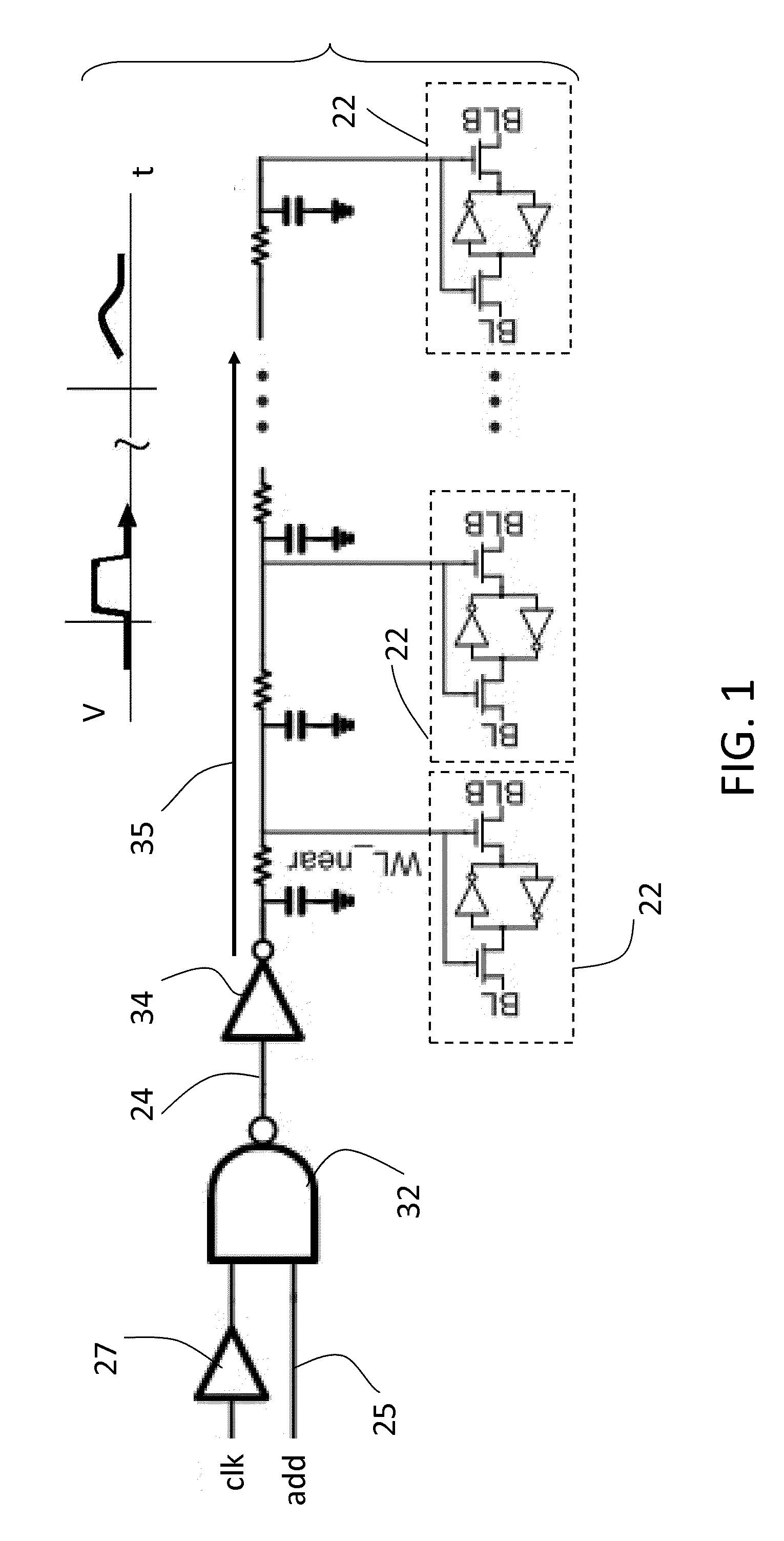
[0030]In FIG. 1, a signal line in an integrated circuit or the like is coupled to a plurality of load devices 22 disposed successively along a signal path. In this example the load devices 22 are shown as bit cells typical of a static random access memory. The signal path in this example corresponds to a word line by which all the bit cells along the signal path are enabled so that the bit cells can be accessed substantially simultaneously over bit lines coupled to each bit cell.

[0031]In the configuration shown, a pulse is produced at a signal source line 24, when the line is addressed by an associated gate input 25 and clock or strobe pulse from a driver 27 at the input to NAND gate 32. The output of gate 32 is coupled to an inverter 34 that drives the signal conduct coupled by successive conductor legs to the word line inputs of the load devices 22.

[0032]At each load device, the word line signal is coupled to the gates of NMOS passing gate field effect transistors (FETs) and the t...


PUM


Abstract

The propagation delay of a signal through multiple load devices coupled sequentially along a conductor is improved by separating a subset of the load devices that is more distant from the signal source, and coupling the more distant subset to the signal through a fly-over conductor that bypasses the subset that is nearer to the signal source. The technique is applicable to subsets of bit cells in a random access memory (SRAM) coupled to a given word line, or to word line decoder gates coupled sequentially to a strobe signal, as well as other circuits wherein load devices selectable as a group can be divided into subsets by proximity to the signal source. In an SRAM layout with multiple levels, different metal deposition layers carry the conductor legs between the load devices versus the fly-over conductor bypassing the nearer subset.

Description

BACKGROUND[0001]This disclosure concerns improving the propagation speed and pulse shape of digital signals propagating in an integrated circuit laid out such that successive loads are located at incremental distances down a signal line coupled at a near end to a signal source. Such a configuration is exemplified by the addressing and enable signals that address or select bit cells in an integrated circuit memory such as a static random access memory (SRAM). Loads that are more distant down the line from the source are electrically isolated from the nearer loads by a gap provided along the signal line, forming two or more discrete subsets of the loads. The signal line is configured with two or more conductors, one being a fly-over conductor that bypasses the nearer loads and couples the more distant loads to the signal source or to a point more proximal to the source.[0002]Integrated circuits may have a succession of load devices connected commonly to a same signal line. The signal ...

Claims


Application Information

Patent Timeline
Patent Type & Authority Applications(United States)
IPC IPC(8): G11C11/00H02J1/00H03H11/26G11C7/00
CPCG11C11/413G11C5/063
Inventor LU, HSIAO-WENHSIEH, WEI-JERCHENG, CHITINGCHOU, CHUNG-CHENGCHANG, JONATHAN TSUNG-YUNG
Owner TAIWAN SEMICON MFG CO LTD
Learn More