Compound semiconductors and their application
a technology of compound semiconductors and semiconductors, applied in the direction of nickel compounds, oxide conductors, non-metal conductors, etc., can solve the problems that many conventional compound semiconductors fail to meet all of these conditions at once, and achieve good thermoelectric conversion performance, low thermal conductivity, and high electric conductivity
- Summary
- Abstract
- Description
- Claims
- Application Information
AI Technical Summary
Benefits of technology
Problems solved by technology
Method used
Image
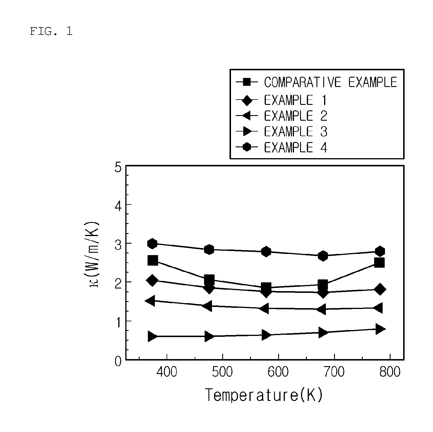
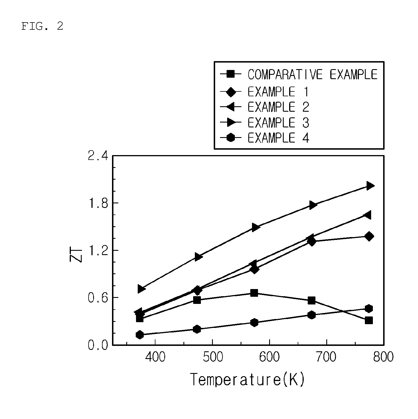
Examples
example 1
[0077]In, Co and Sb were prepared as reagents, and were mixed by using mortar to make a mixture having a composition of In0.25Co4Sb11 in a pellet form. The mixture was heated at 500° C. for 15 hours under H2 (1.94%) and N2 gas. The time for raising the temperature to 500° C. was 1 hour and 30 minutes.
[0078]Next, Te was added to In0.25Co4Sb11 as a reagent to make an In0.25Co4Sb11Te1 mixture. The mixture was prepared in a glove bag filled with Ar.
[0079]The materials mixed as above were put into a silica tube and vacuum-sealed and then heated at 650° C. for 36 hours. The time for raising the temperature to 650° C. was 1 hour and 30 minutes, and In0.25Co4Sb11Te1 powder was obtained.
[0080]A part of the composed materials prepared above was formed into a cylinder having a diameter of 4 mm and a length of 15 mm, and another part was formed into a disk having a diameter of 10 mm and a thickness of 1 mm. After that, a pressure of 200 MPa was applied thereto by using a CIP (Cold Isostatic Pre...
example 2
[0083]In, Co and Sb were prepared as reagents, and were mixed by using mortar to make a mixture having compositions of In0.25Co4Sb10 and In0.25Co4Sb11 in a pellet form. The mixture was heated at 500° C. for 15 hours under H2 (1.94%) and N2 gas. The time for raising the temperature to 500° C. was 1 hour and 30 minutes.
[0084]Next, Te was added to In0.25Co4Sb10 as a reagent to make an In0.25Co4Sb10Te2 mixture. In addition, this mixture was suitably mixed with the In0.25Co4Sb11 to make an In0.25Co4Sb10.75Te1.25 mixture. The mixture was prepared in a glove bag filled with Ar.
[0085]The materials mixed as above were put in a silica tube and vacuum-sealed, and then were heated at 650° C. for 36 hours. The time for raising the temperature to 650° C. was 1 hour and 30 minutes, and In0.25Co4Sb10.75Te1.25 powder was obtained.
[0086]A part of the material prepared above was formed into a cylinder having a diameter of 4 mm and a length of 15 mm, and another part was formed into a disk having a dia...
example 3
[0089]In, Co and Sb were prepared as reagents, and were mixed by using mortar to make a mixture having compositions of In0.25Co4Sb10 and In0.25Co4Sb11 in a pellet form. The mixture was heated at 500° C. for 15 hours under H2 (1.94%) and N2 gas. The time for raising the temperature to 500° C. was 1 hour and 30 minutes.
[0090]Next, Te was added to In0.25Co4Sb10 as a reagent to make an In0.25Co4Sb10Te2 mixture. In addition, the mixture was suitably mixed with the In0.25Co4Sb11 to make an In0.25Co4Sb10.5Te1.5 mixture. The mixture was prepared in a glove bag filled with Ar.
[0091]The materials mixed as above were put into a silica tube and vacuum-sealed and then heated at 650° C. for 36 hours. Here, the temperature rising time was 1 hour and 30 minutes, and In0.25Co4Sb10.5Te1.5 powder was obtained.
[0092]A part of the material prepared above was formed into a cylinder having a diameter of 4 mm and a length of 15 mm, and another part was formed into a disk having a diameter of 10 mm and a th...
PUM
| Property | Measurement | Unit |
|---|---|---|
| temperature | aaaaa | aaaaa |
| temperature | aaaaa | aaaaa |
| temperature | aaaaa | aaaaa |
Abstract
Description
Claims
Application Information
 - R&D
- Intellectual Property
- Life Sciences
- Materials
- Tech Scout
- Unparalleled Data Quality
- Higher Quality Content
- 60% Fewer Hallucinations
Browse by: Latest US Patents, China's latest patents, Technical Efficacy Thesaurus, Application Domain, Technology Topic, Popular Technical Reports.
© 2025 PatSnap. All rights reserved.Legal|Privacy policy|Modern Slavery Act Transparency Statement|Sitemap|About US| Contact US: help@patsnap.com


