Method of depositing gate dielectric, method of preparing mis capacitor, and mis capacitor

a gate dielectric and capacitor technology, applied in the field of semiconductor devices, can solve the problems of low dielectric, limited properties of ultra-thin siosub>2 /sub>gate dielectric layers, and unavoidable low dielectric, so as to reduce the equivalent oxide thickness and improve electrical properties.

Inactive Publication Date: 2012-11-01
SHANGHAI INST OF MICROSYSTEM & INFORMATION TECH CHINESE ACAD OF SCI
View PDF3 Cites 10 Cited by
  • Summary
  • Abstract
  • Description
  • Claims
  • Application Information

AI Technical Summary

Benefits of technology

The invention provides a method of depositing a gate dielectric using a plasma-enhanced atomic layer deposition process. The method includes preprocessing the surface of a semiconductor substrate with oxygen plasma and nitrogen-containing plasma to form a nitrogen-containing oxide layer, which acts as a buffer layer during the growth of a high-k gate dielectric layer. This results in a reduction in equivalent oxide thickness and improved electrical properties. Additionally, the invention provides a method of preparing an MIS capacitor by depositing a buffer layer and a gate dielectric layer, followed by the formation of a metal electrode on both surfaces of the substrate. The MIS capacitor includes a semiconductor substrate, a buffer layer, and a gate dielectric layer arranged between two metal electrodes. The technical effects of the invention include improved performance and reliability of semiconductor devices.

Problems solved by technology

However, when a thickness of the SiO2 gate oxide layer is less than 1 nm, a leakage current caused by direct tunneling effect may become high enough to induce device failure.
And moreover, an ultra-thin SiO2 gate dielectric layer is limited in properties such as its long-term reliability, boron penetration, and uniformity.
However, the HfO2 film grown by the conventional ALD process or PEALD process and its substrate have an unavoidable low dielectric-constant SiO2 layer sandwiched therebetween, and the SiO2 layer grows further during an annealing process.
In addition, the HfO2 film usually has lots of oxygen vacancies contained therein, resulting in an increase in equivalent oxide thickness (abbreviated as EOT) and deterioration in electrical properties.

Method used


Image

  • Method of depositing gate dielectric, method of preparing mis capacitor, and mis capacitor
  • Method of depositing gate dielectric, method of preparing mis capacitor, and mis capacitor

Examples


Embodiment Construction

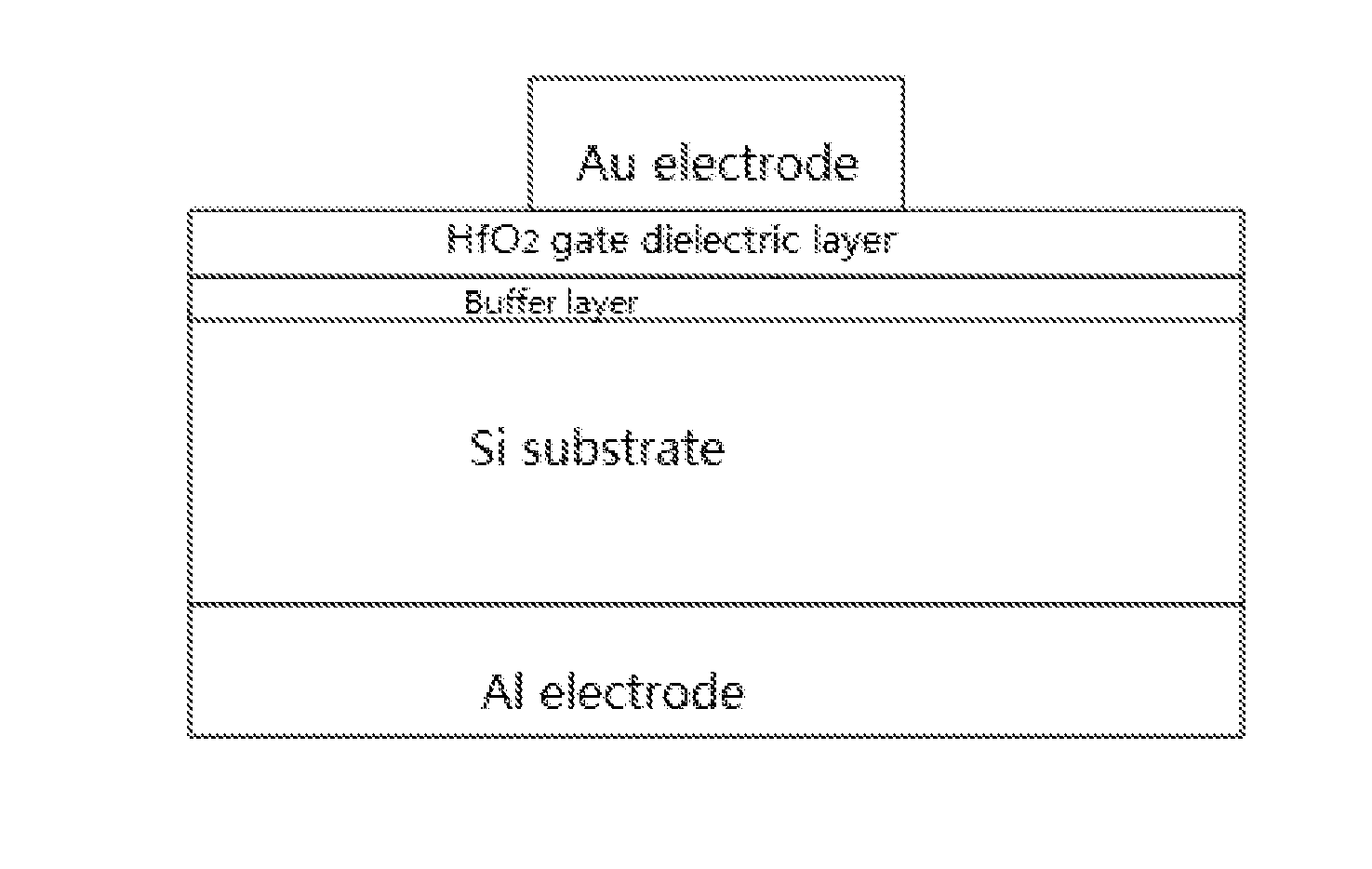
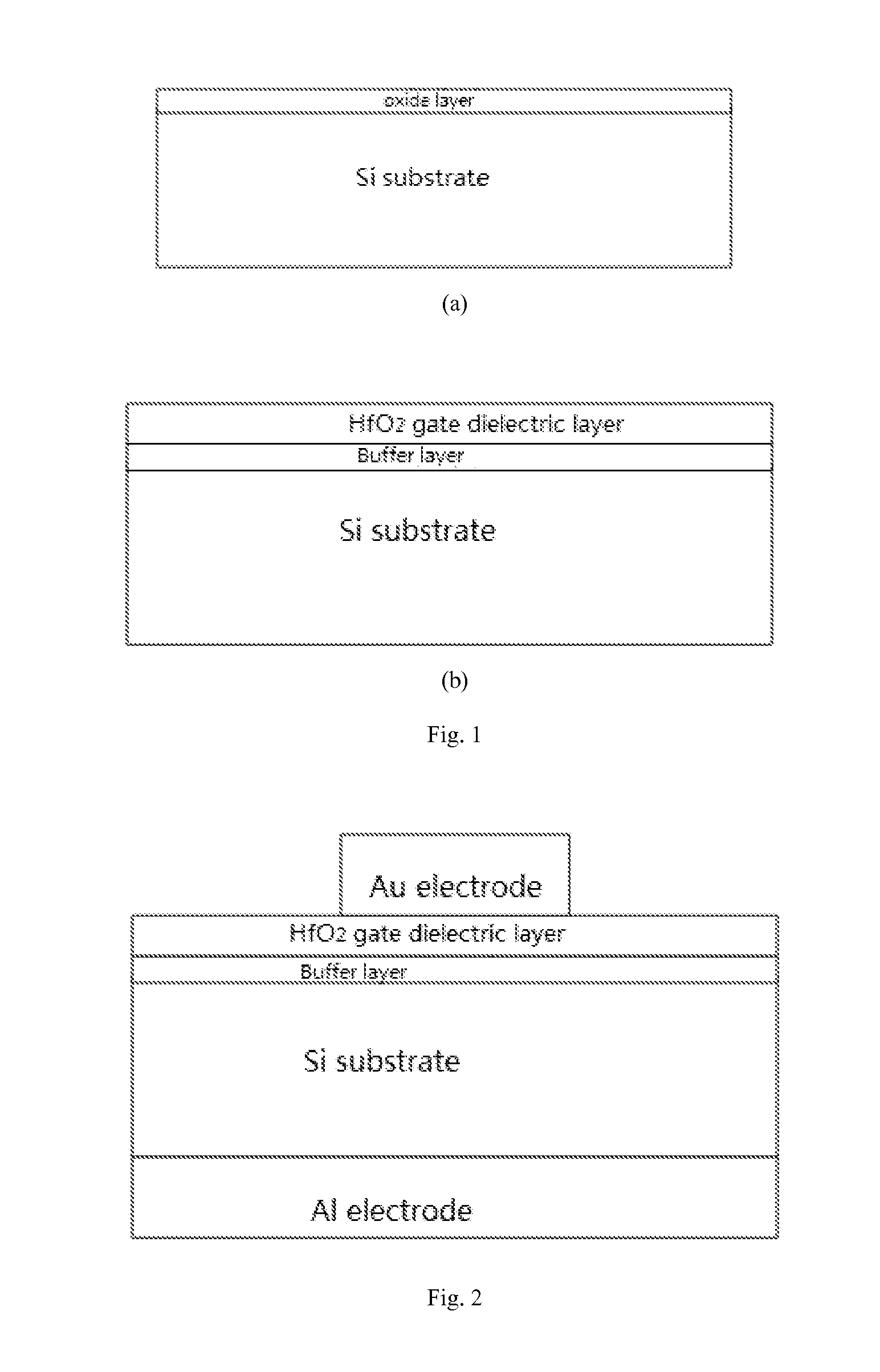
[0014]Now referring to the drawings, the present invention is described in detail as below.

[0015]A method of depositing a gate dielectric by a plasma-enhanced atomic layer deposition process of the present invention comprises the following steps.

[0016]Firstly, a semiconductor substrate is subjected to a cleaning process. For example, a well-cut Si substrate is put into a solution (NH4OH:H2O2:H2O=2:1:7 in volume ratio) to be ultrasonically washed for 15 minutes so as to remove metal pollutants resided on a surface thereof and is further rinsed with deionized water, followed by being kept in a diluted HF solution (HF:H2O=1:50 in volume ratio) for about 3 minutes to remove a surface oxide resided on the Si substrate. Subsequently, the surface of the Si substrate is rinsed again with deionized water, and then is dewatered with alcohol to complete the cleaning process.

[0017]Next, the surface of the cleaned semiconductor substrate is preprocessed with oxygen plasma and nitrogen-containing...


PUM


Abstract

The present invention relates to a method of depositing a gate dielectric, a method of preparing a MIS capacitor and the MIS capacitor. In the method of depositing the gate dielectric, a semiconductor substrate surface is preprocessed with oxygen plasma and nitrogen-containing plasma to form a nitrogen-containing oxide layer thereon. Then, a high-k gate dielectric layer is grown on the nitrogen-containing oxide layer surface by a plasma-enhanced atomic layer deposition process, and the oxide layer converts during the gate dielectric layer growth process into a buffer layer of a dielectric constant higher than SiO2. Then, a metal electrode is formed on both an upper layer and a lower layer of the thus-formed semiconductor construction, so that a MIS capacitor is prepared. According to the present invention, the formation of the buffer layer enables the interface characteristics between semiconductor materials and high-k gate dielectric layers to be improved effectively, equivalent oxide thickness (EOT) to be reduced and electrical properties to be enhanced.

Description

FIELD OF THE INVENTION[0001]The present invention relates to a semiconductor field, and more particularly to a method of depositing a gate dielectric, to a method of preparing a MIS capacitor and to the MIS capacitor.BACKGROUND OF THE INVENTION[0002]A SiO2 gate dielectric layer has become thinner and thinner with the rapid development of microelectronic technology. However, when a thickness of the SiO2 gate oxide layer is less than 1 nm, a leakage current caused by direct tunneling effect may become high enough to induce device failure. And moreover, an ultra-thin SiO2 gate dielectric layer is limited in properties such as its long-term reliability, boron penetration, and uniformity. Presently, one of the effective ways to overcome the above limitations is to utilize a new insulation dielectric material (high-k material) of a high dielectric constant. Utilizing the high-k material may lead to an increase in the thickness of the gate dielectric layer with the control over channels en...

Claims


Application Information

Patent Timeline
Patent Type & Authority Applications(United States)
IPC IPC(8): H01L29/94H01L21/334H01L21/3105
CPCH01L21/02181H01L21/022H01L21/02238H01L21/02274H01L21/0228H01L21/02304H01L29/518H01L21/0234H01L28/40H01L21/28194H01L21/28202H01L29/513H01L29/517H01L21/02332
Inventor CHENG, XINHONGXU, DAWEIWANG, ZHONGJIANXIA, CHAOHE, DAWEISONG, ZHAORUIYU, YUEHUI
Owner SHANGHAI INST OF MICROSYSTEM & INFORMATION TECH CHINESE ACAD OF SCI
Why Eureka
Try Eureka