Ceramic material, member for semiconductor manufacturing equipment, sputtering target member and method for producing ceramic material

Active Publication Date: 2012-09-13
NGK INSULATORS LTD
View PDF3 Cites 18 Cited by
  • Summary
  • Abstract
  • Description
  • Claims
  • Application Information

AI Technical Summary

Benefits of technology

[0007]However, magnesium oxide reacts with moisture and carbon dioxide in air to form hydroxide and carbonate. Thus, the surface of magnesium oxide is gradually altered (problem of moisture resistance). In the case where magnesium oxide is used for a member for semiconductor manufacturing equipment, hydroxide and carbonate are disadvantageously decomposed to form gases, so that magnesium oxide is formed into particles, thereby emitting particles to contaminate a semiconductor device. Thus, application of magnesium oxide has been limited. To improve moisture resistance, there is a method in which NiO, ZnO, and so forth form a solid solution with magnesium oxide (PTL 2). These metal components, however, serve as contaminants that affect the properties of a semiconductor device. Thus, these metal components are not preferred as additives.
[0012]The inventors have conducted intensive studies on the corrosion resistance of a ceramic material formed by compacting a mixed powder of magnesium oxide, alumina, and aluminum nitride and subjecting the resulting compact to hot-press sintering and have found that a ceramic material having a crystal phase of a MgO—AlN solid solution in which aluminum and nitrogen components are dissolved in magnesium oxide, the crystal phase serving as a main phase, is excellent in corrosion resistance, moisture resistance, and water resistance. These findings have led to the completion of the present invention.
[0017]The ceramic material of the present invention has corrosion resistance comparable to magnesium oxide and has superior moisture resistance and water resistance to magnesium oxide. Thus, a member composed of the ceramic material for semiconductor manufacturing equipment can withstand a high-reactive halogen (e.g., F or Cl)-based plasma used in a semiconductor fabrication process for prolonged periods of time and can reduce the amount of particles emitted from the member. Furthermore, the member has high moisture resistance and water resistance and is not easily altered, compared with common magnesium oxide. Thus, the member can be wet-processed.
[0019]As described above, the ceramic material has higher moisture resistance than common magnesium oxide and thus is not easily altered. When the ceramic material is transferred and handled in air, hydroxide and carbonate are not easily formed on the surface. It is thus possible to reduce contamination with gas components formed by the decomposition of hydroxide and carbonate at the time of, for example, sputtering for the production of a MTJ device. Furthermore, it is possible to reduce the effect on a material on which a film is to be formed. Thereby, a magnetic tunnel junction device having higher performance should be provided.

Problems solved by technology

Thus, the surface of magnesium oxide is gradually altered (problem of moisture resistance).
In the case where magnesium oxide is used for a member for semiconductor manufacturing equipment, hydroxide and carbonate are disadvantageously decomposed to form gases, so that magnesium oxide is formed into particles, thereby emitting particles to contaminate a semiconductor device.
Thus, application of magnesium oxide has been limited.
These metal components, however, serve as contaminants that affect the properties of a semiconductor device.

Method used


Image

  • Ceramic material, member for semiconductor manufacturing equipment, sputtering target member and method for producing ceramic material
  • Ceramic material, member for semiconductor manufacturing equipment, sputtering target member and method for producing ceramic material
  • Ceramic material, member for semiconductor manufacturing equipment, sputtering target member and method for producing ceramic material

Examples


examples

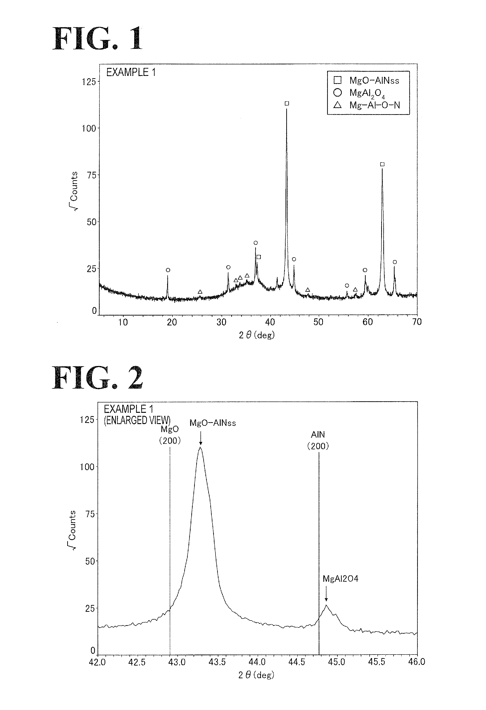
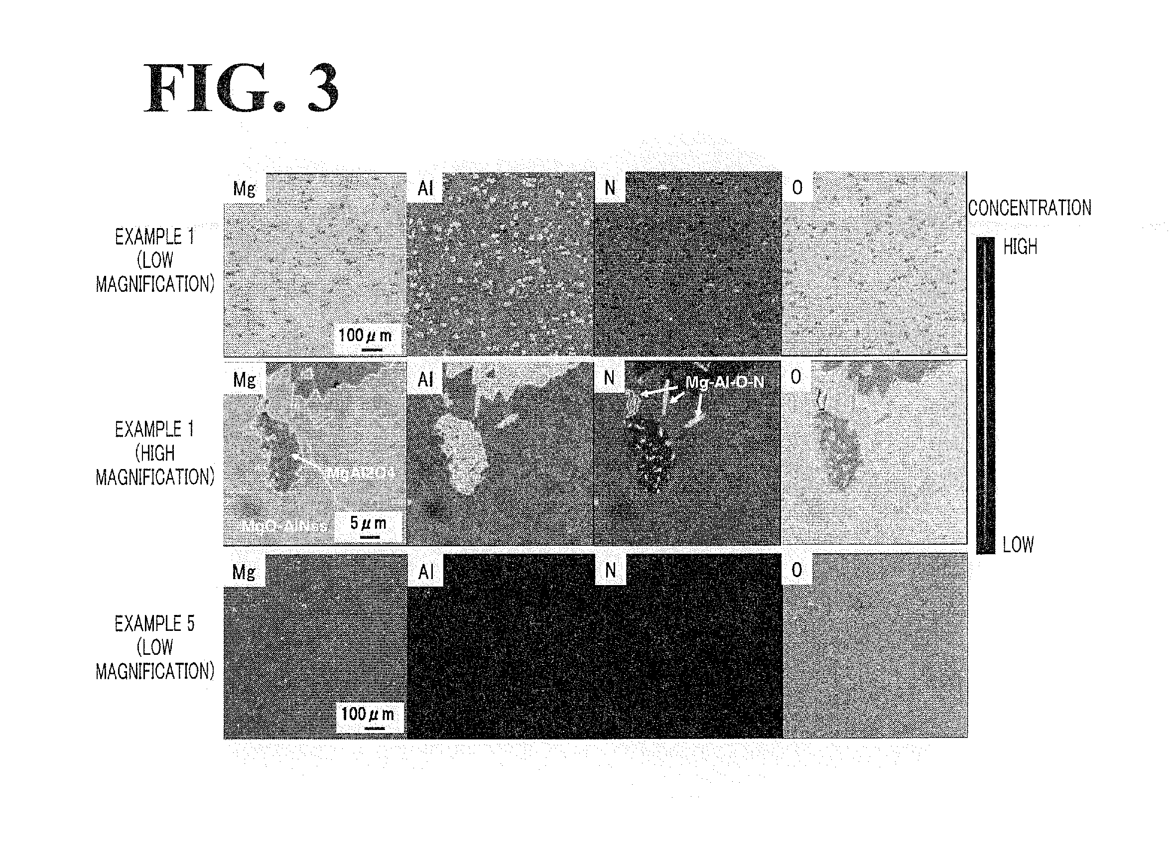
[0035]Preferred application examples of the present invention will be described below. In Experimental Examples 1 to 16, as raw material MgO, raw material Al2O3, and raw material AlN, commercial items each having a purity of 99.9% by mass or more and an average particle size of 1 μm or less were used. In Experimental Examples 17 to 28, a commercial item having a purity of 99.4% by mass and an average particle size of 3 μm was used as raw material MgO, a commercial item having a purity of 99.9% by mass and an average particle size of 0.5 μm was used as raw material Al2O3, and a commercial item, having an average particle size of 1 μm or less, the same as that used in Experimental Examples 1 to 16 was used as raw material AlN. Here, with respect to raw material AlN, an oxygen contamination of about 1% by mass is inevitable. Thus, the foregoing purity is a value of impurity elements excluding oxygen. Experimental Examples 1 to 4, 7 to 17, 21, and 23 to 28 correspond to examples of the ...

experimental examples 1 to 3

Preparation

[0036]Raw material MgO, raw material Al2O3, and raw material AlN were weighed in amounts (% by mass) described in Table 1. These materials were wet-mixed for 4 hours in a nylon pot with alumina balls each having a diameter of 5 mm using isopropyl alcohol as a solvent. After the completion of the mixing, the resulting slurry was taken out and dried at 110° C. in a stream of nitrogen. Then the mixture was passed through a 30-mesh sieve to provide a mixed powder. The ratio by mole of Mg / Al of the mixed powder was 2.9.

Compacting

[0037]The mixed powder was subjected to uniaxial pressing at 200 kgf / cm2 to form a disk-like formed article having a diameter of about 35 mm and a thickness of about 10 mm. The formed article was accommodated in a graphite mold for sintering.

Sintering

[0038]The disk-like formed article was subjected to hot-press sintering to provide a ceramic material. The hot-press sintering was performed at a pressing pressure of 200 kgf / cm2 and a sintering temperatur...

experimental example 4

[0039]A ceramic material was prepared as in Experimental Example 1, except that the sintering temperature was 1650° C.


PUM

PropertyMeasurementUnit
Percent by massaaaaaaaaaa

Abstract

A ceramic material according to the present invention mainly contains magnesium, aluminum, oxygen, and nitrogen, the ceramic material has the crystal phase of a MgO—AlN solid solution in which aluminum nitride is dissolved in magnesium oxide, the crystal phase serving as a main phase. Preferably, XRD peaks corresponding to the (200) and (220) planes of the MgO—AlN solid solution measured with CuKα radiation appear at 2θ=42.9 to 44.8° and 62.3 to 65.2°, respectively, the XRD peaks being located between peaks of cubic magnesium oxide and peaks of cubic aluminum nitride. More preferably, the XRD peak corresponding to the (111) plane appears at 2θ=36.9 to 39°, the XRD peak being located between a peak of cubic magnesium oxide and a peak of cubic aluminum nitride.

Description

TECHNICAL FIELD[0001]The present invention relates to a ceramic material, a member for use in semiconductor manufacturing equipment, a sputtering target member, and a method for producing a ceramic material.BACKGROUND ART[0002]In semiconductor manufacturing equipment used for dry processes, plasma coating, and so forth in semiconductor manufacturing, a high-reactivity halogen (e.g., F or Cl)-based plasma is used for etching and cleaning. Thus, members used in the semiconductor manufacturing equipment are required to have high corrosion resistance. In general, high-corrosion resistant metals, such as anodized aluminum and Hastelloy, and ceramic members are used. In particular, materials for electrostatic chucks, which support Si wafers, and heaters are required to have high corrosion resistance and low particle emission properties. Thus, high-corrosion resistant ceramic members composed of, for example, aluminum nitride, alumina, sapphire, are used. Long-term use of these materials c...

Claims


Application Information

Patent Timeline
IPC IPC(8): C04B35/04C23C14/06C23C14/34C04B35/645
CPCC04B35/581H01L21/6833C04B35/6261C04B35/62655C04B35/645C04B2235/3206C04B2235/3217C04B2235/3222C04B2235/3865C04B2235/3869C04B2235/5445C04B2235/762C04B2235/77C04B2235/80C04B2235/96C04B2235/9669C23C14/3414C04B35/58C04B35/04H01L21/3065H01L21/31
Inventor WATANABE, MORIMICHIJINDO, ASUMIKATSUDA, YUJISATO, YOSUKEISODA, YOSHINORI
Owner NGK INSULATORS LTD
Why Eureka
Try Eureka