Photoelectric element
a photoelectric element and electron transport layer technology, applied in the field of photoelectric elements, can solve the problems of insufficient conversion efficiency, difficult further improvement of conversion efficiency, and insufficient conversion efficiency, so as to improve the electron transport property of the electron transport layer and improve the conversion efficiency of the photoelectric elemen
- Summary
- Abstract
- Description
- Claims
- Application Information
AI Technical Summary
Benefits of technology
Problems solved by technology
Method used
Image
Examples
example 1
Synthesis of Galvi Monomer
[0151]Into a reaction container, 4-bromo-2,6-di-tert-butyl phenol (135.8 g; 0.476 mol) and acetonitrile (270 ml) were introduced, furthermore, under inert atmosphere, N,O-bis (trimethylsilyl)acetamide (BSA) (106.3 g; 129.6 ml) was added, which were stirred overnight at 70° C. and reacted until crystals were deposited completely. The deposited white crystals were filtered, vacuum-dried and then re-crystallized with ethanol for purification to obtain a white plate crystal of (4-bromo-2,6-di-tert-butyl phenoxy)trimethylsilane (150.0 g; 0.420 mol) indicated by the symbol “1” in [Chem. 35].
[0152]Next, in the reaction container, under inert atmosphere, the above (4-bromo-2,6-di-tert-butyl phenoxy)trimethylsilane (9.83 g; 0.0275 mol) was dissolved in tetrahydrofuran (200 ml), and the prepared solution was cooled to −78° C. using dry ice / methanol. Added to this solution inside the reaction container was 1.58 M of n-butyl lithium / hexane solution (15.8 ml; 0.025 mol)...
example 2
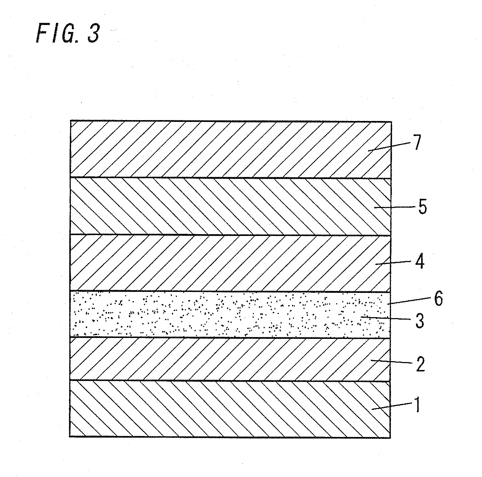
[0166]In Example 1, when forming the electron transport layer 3, 0.2 g of galvi polymer and 0.01 g of sensitizing dye (D131) were dissolved in 10 ml of chlorobenzene to prepare a coating solution. This solution was spincoated at 2,000 rpm over the first electrode 2 of an electro-conductive glass substrate and dried under 60° C. and 0.01 MPa for one hour thereby forming an electron transport layer 3 having a thickness of 60 nm. Immersion of this electron transport layer 3 into a saturated acetonitrile solution of sensitizing dye was not carried out.
[0167]A photoelectric element was prepared in a similar manner to Example 1 except for this.
example 3
[0168]In Example 1, after the electron transport layer 3 was formed, this electron transport layer 3 was immersed in an aqueous solution of tetrabutyl ammonium at a concentration of 0.1 M for 15 minutes thereby anionizing the galvi polymer constituting the electron transport layer 3. This electron transport layer 3 was washed with water and then immersed in an aqueous solution of polydecylviologen (ph 10) at a concentration of 0.1 M for 15 minutes thereby bonding the polydecylviologen electrostatically to the anionized galvi polymer.
[0169]Next, this electron transport layer 3 was immersed in an acetonitrile solution containing the sensitizing dye (D131) at a concentration of 0.3 mM for one hour and then washed with water. In this way, the sensitizing dye was electrostatically bonded to the portion derived from polydecylviologen, which is a substance that is positively charged in the electron transport layer 3.
[0170]In addition, as the electrolytic solution, an acetonitrile solution ...
PUM
| Property | Measurement | Unit |
|---|---|---|
| Diameter | aaaaa | aaaaa |
| Diameter | aaaaa | aaaaa |
| Porosity | aaaaa | aaaaa |
Abstract
Description
Claims
Application Information
 - R&D
- Intellectual Property
- Life Sciences
- Materials
- Tech Scout
- Unparalleled Data Quality
- Higher Quality Content
- 60% Fewer Hallucinations
Browse by: Latest US Patents, China's latest patents, Technical Efficacy Thesaurus, Application Domain, Technology Topic, Popular Technical Reports.
© 2025 PatSnap. All rights reserved.Legal|Privacy policy|Modern Slavery Act Transparency Statement|Sitemap|About US| Contact US: help@patsnap.com


