
Plasma processing apparatus and method of producing amorphous silicon thin film using same

a technology of plasma processing and amorphous silicon thin film, which is applied in the direction of sustainable manufacturing/processing, final product manufacturing, coatings, etc., can solve the problems that the exhaust and the disclosed gas suction hole cannot be considered to be able to sufficiently exhibit the capability, etc., to achieve efficient removal of unwanted materials, reduce the effect of structural defects and few defects

Inactive Publication Date: 2012-05-10
TORAY IND INC
View PDF2 Cites 17 Cited by
  • Summary
  • Abstract
  • Description
  • Claims
  • Application Information

AI Technical Summary

Benefits of technology

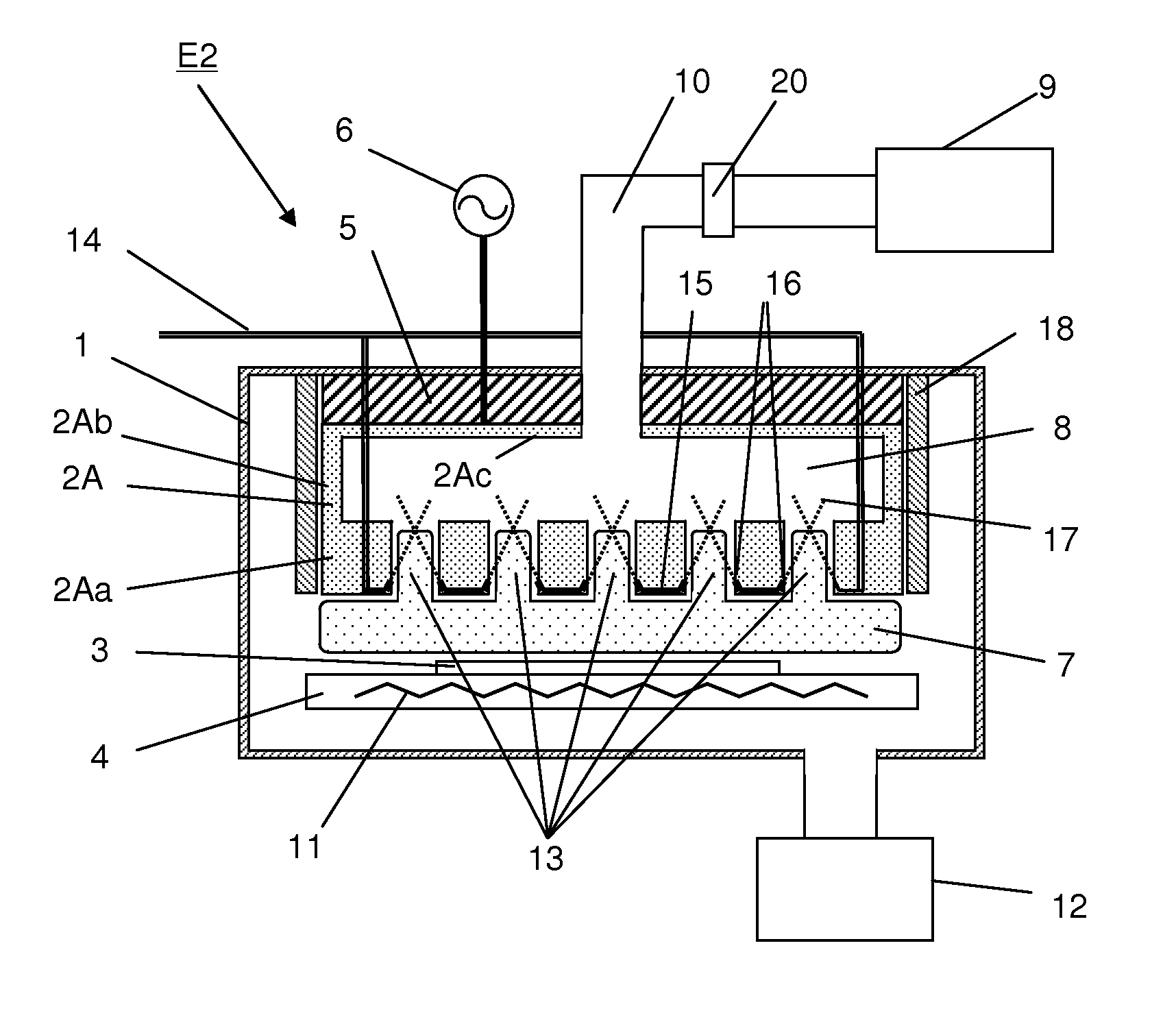
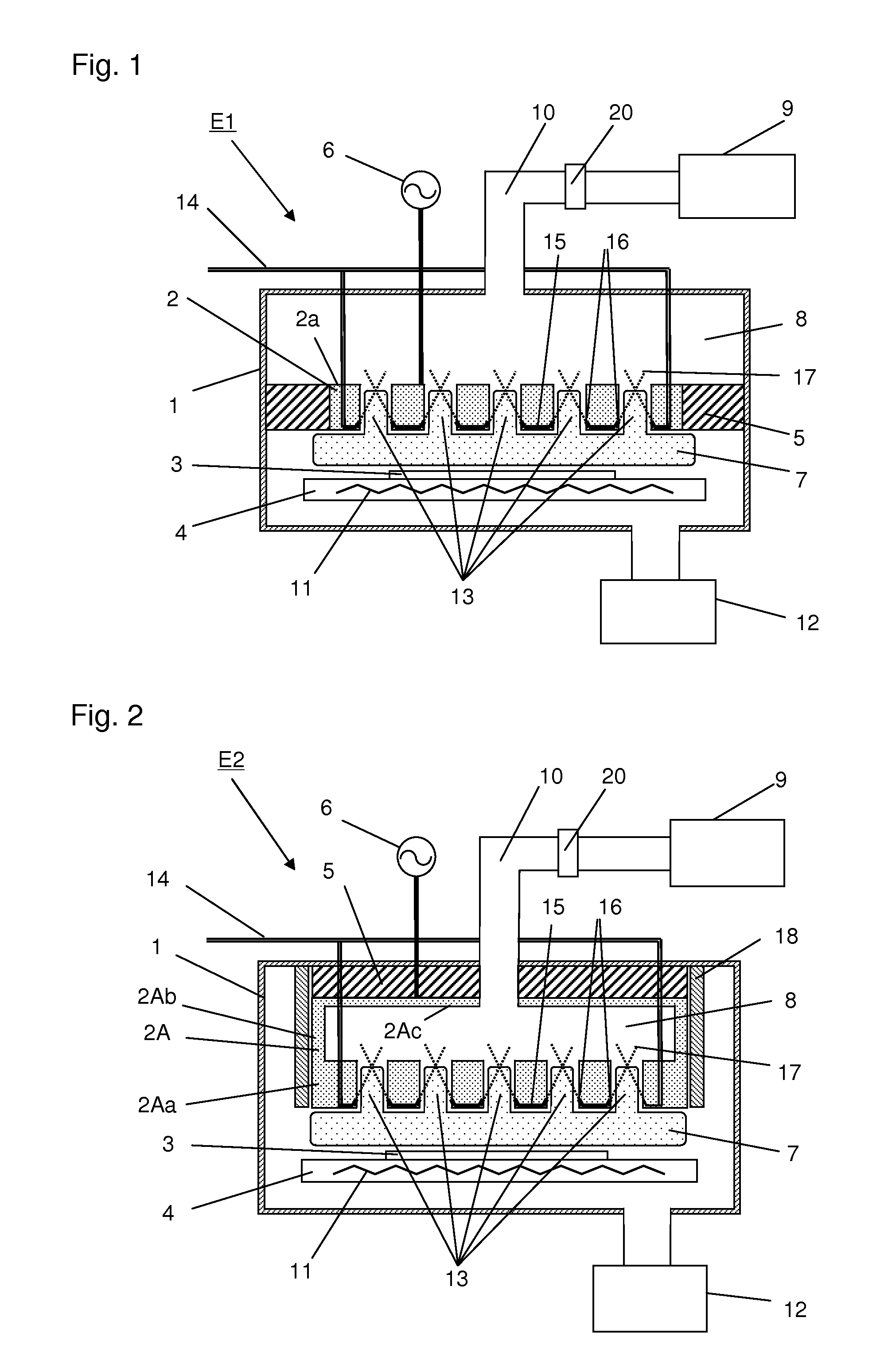
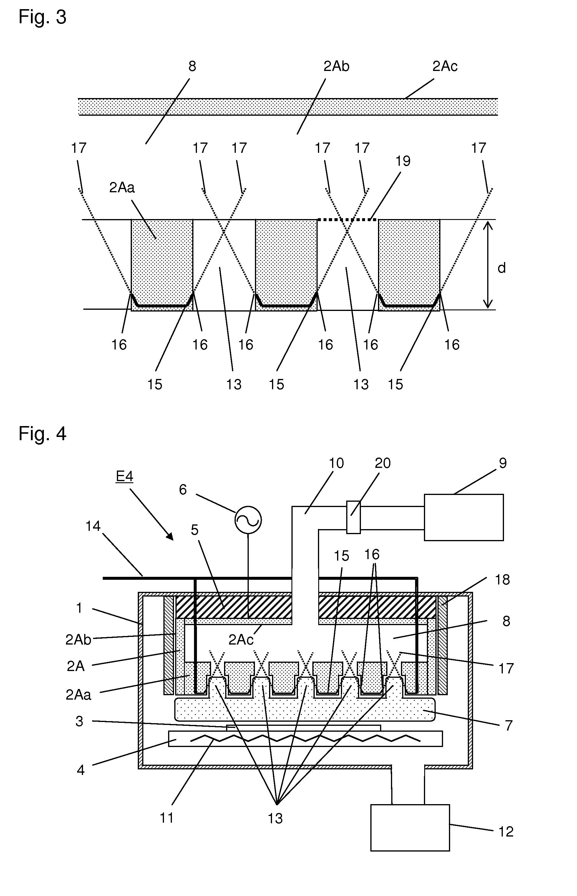
[0018]The invention provides a plasma processing apparatus capable of efficiently removing the unwanted materials generated in plasma processing, and also provides a method for producing a high-quality amorphous silicon thin-film small in the amount of unwanted materials such as higher silanes and particles mixed into the film, by the chemical vapor deposition (CVD) using a plasma by using the plasma processing apparatus.
[0040]The invention provides a plasma processing apparatus capable of efficiently removing the unwanted materials generated by plasma processing. If the plasma processing apparatus of the invention is used as plasma CVD apparatus, the film can be formed in such an environment where unwanted materials of high molecular weights, particles and the like are prevented from being mixed into the formed film, and consequently a high-quality thin-film having few defects can be obtained. The amorphous silicon thin-film produced by using the plasma CVD apparatus is a thin film having few structural defects and little light induced degradation, since unwanted materials such as higher silanes and particles are sufficiently prevented from being mixed into the film. If the amorphous silicon thin-film is used in a solar cell, the decline of the obtained solar cell in conversion efficiency due to light induced degradation can be decreased.

Problems solved by technology

Accordingly the disclosed numerous exhaust holes cannot be considered to be able to sufficiently exhibit the capability of removing the unwanted materials by the exhaust from the electrode.
Therefore, the disclosed gas suction holes cannot be considered to be able to sufficiently exhibit the capability of removing the unwanted materials by the exhaust from the electrode as in the case of Patent Literature 1.

Method used


Image

  • Plasma processing apparatus and method of producing amorphous silicon thin film using same
  • Plasma processing apparatus and method of producing amorphous silicon thin film using same
  • Plasma processing apparatus and method of producing amorphous silicon thin film using same

Examples


example 1

[0113]The plasma processing apparatus E4 shown in FIGS. 4 and 5 was used to form an amorphous silicon thin-film on a substrate on the basis of the abovementioned first embodiment for forming an amorphous silicon thin-film, and the Si—H2 bond concentration of the formed thin-film was obtained. The quality of the formed thin-film was evaluated on the basis of the concentration.

[0114]As the substrate 3, monocrystalline silicon was used. The substrate 3 was set on the substrate holding mechanism 4, and the substrate heating mechanism 11 was used to heat the substrate 3 to a temperature of 220° C. The auxiliary gas exhaust device 12 was used to exhaust the gas in the vacuum vessel 1 till the pressure in the vacuum vessel 1 became 1×10⁻⁴ Pa or less, and subsequently the operation of exhausting the gas in the vacuum vessel 1 was switched from the auxiliary gas exhaust device 12 to the gas exhaust device 9. As the source gas, 300 sccm of silane gas was introduced from the gas introduction p...

example 2

[0121]An amorphous silicon thin-film was formed on a substrate using the plasma processing apparatus E6 shown in FIGS. 6 and 7 on the basis of the abovementioned second embodiment for forming an amorphous silicon thin-film, according to the same procedure as that in Example 1. The Si—H2 bond concentration of the formed amorphous silicon thin-film was calculated on the basis of the same method as that of Example 1. As a result, the Si—H2 bond concentration of the formed amorphous silicon thin-film was 0.6%, and it was confirmed that the amorphous silicon thin-film was low in the defect density thereof.

example 3

[0122]An amorphous silicon thin-film was formed on a substrate according to the same procedure as that of Example 1, except that the plasma processing apparatus E8 shown in FIGS. 8 and 9 was used on the basis of the abovementioned third embodiment for forming an amorphous silicon thin-film, and that power of 80 W was supplied to the plasma generating electrode 2A. The Si—H2 bond concentration of the formed amorphous silicon thin-film was calculated on the basis of the same method as that of Example 1. As a result, the Si—H2 bond concentration of the formed amorphous silicon thin-film was 0.3%, and it was confirmed that the formed amorphous silicon thin-film was low in the defect density thereof.


PUM

PropertyMeasurementUnit
Pressureaaaaaaaaaa

Abstract

Disclosed is a plasma processing apparatus, wherein a plasma-generating electrode has a plurality of gas exhaust holes which run through the plasma-generating electrode from the surface facing a substrate held by a substrate-holding mechanism, and reach a gas exhaust chamber; gas-feeding pipes, provided connected to a gas-introducing pipe, have gas-feeding ports for discharging source gas toward the inside of the plurality of gas exhaust holes; and the gas-feeding pipes and the gas-feeding ports are arranged in a manner such that extended lines, representing the direction of the flow of the source gas discharged from the gas-feeding ports, intersect the end surface open regions at the interface of the gas exhaust chamber to the gas exhaust holes. Also disclosed is a method of producing the amorphous silicon thin film using the plasma processing apparatus.

Description

CROSS-REFERENCE TO RELATED APPLICATIONS[0001]This application is the U.S. National Phase application of PCT International Application No. PCT / JP2010 / 054293, filed Mar. 15, 2010, and claims priority to Japanese Patent Application No. JP 2009-071385, filed Mar. 24, 2009, the disclosures of which PCT and priority applications are incorporated herein by reference in their entirely for all purposes.FIELD OF THE INVENTION[0002]The present invention relates to a plasma processing apparatus, particularly a plasma CVD apparatus for forming a thin film by chemical vapor deposition (CVD) using a plasma, and a method for producing an amorphous silicon thin-film using the apparatus.BACKGROUND OF THE INVENTION[0003]In recent years, under growing awareness of environmental friendliness, photovoltaic power generation attracts attention. In this situation, various solar cells have been developed, and some of them are practically used. Above all, thin-film silicon solar cells that are small in the am...

Claims


Application Information

Patent Timeline
IPC IPC(8): H01L21/20H01L21/3065C23C16/50
CPCC23C16/24C23C16/5096H01J37/3244H01L21/02532H01J37/32541H01L21/02422H01J37/32449C23C16/45565H01J37/32357H01J37/32422H01J37/32834H01J37/32871H01L31/03767H01L31/202Y02P70/50Y02E10/50
Inventor SAKAMOTO, KEITAROMOMURA, FUMIYASUKOMORI, TSUNENORI
Owner TORAY IND INC
Learn More