
Method for manufacturing a group III nitride crystal, method for manufacturing a group III nitride template, group III nitride crystal and group III nitride template

a technology of nitride crystals and manufacturing methods, which is applied in the direction of non-metal conductors, conductors, polycrystalline materials, etc., can solve the problems of filter housing immediate filling, exhaust line clogging in an upstream side of the filter, similar problems, etc., and achieve the effect of suppressing the generation of by-products and suppressing the damage in the reactor comprising quartz

Inactive Publication Date: 2012-05-03
HITACHI CABLE
View PDF1 Cites 6 Cited by
  • Summary
  • Abstract
  • Description
  • Claims
  • Application Information

AI Technical Summary

Benefits of technology

[0041]According to the invention, a method for manufacturing a group III nitride crystal, a method for manufacturing a group III nitride template, a group III nitride crystal and a group III nitride template is provided, in which a damage in a reactor comprising quartz can be suppressed and generation of by-product can be suppressed. Further, it is possible to provide the group III nitride crystal with n-type conductivity, p-type conductivity or semi-insulation property.

Problems solved by technology

However, when a thick film is grown to obtain a single crystal substrate, there are disadvantages in that a filter housing is immediately filled up and that the exhaust line is clogged in an upstream side of the filter.
Further, when an AlxGa1−xN mixed crystal is grown, a similar problem arises although in a smaller degree.
In addition, there is another disadvantage in that, in the HVPE method using the trihalide, the amount of the trihalide to be conveyed as the source material is one-third (⅓) compared with the amount of the hydrogen halide which is supplied to the reactor.
Therefore, this technique is inefficient.
Accordingly, there is a disadvantage in that it is difficult to precisely control the electrical conductivity for providing the group III nitride crystal with a semi-insulating property or p-type conductivity as well as the n-type conductivity.

Method used


Image

  • Method for manufacturing a group III nitride crystal, method for manufacturing a group III nitride template, group III nitride crystal and group III nitride template
  • Method for manufacturing a group III nitride crystal, method for manufacturing a group III nitride template, group III nitride crystal and group III nitride template
  • Method for manufacturing a group III nitride crystal, method for manufacturing a group III nitride template, group III nitride crystal and group III nitride template

Examples


embodiment

[0057]Next, en embodiment according to the invention will be explained in more detail in conjunction with appended drawings.

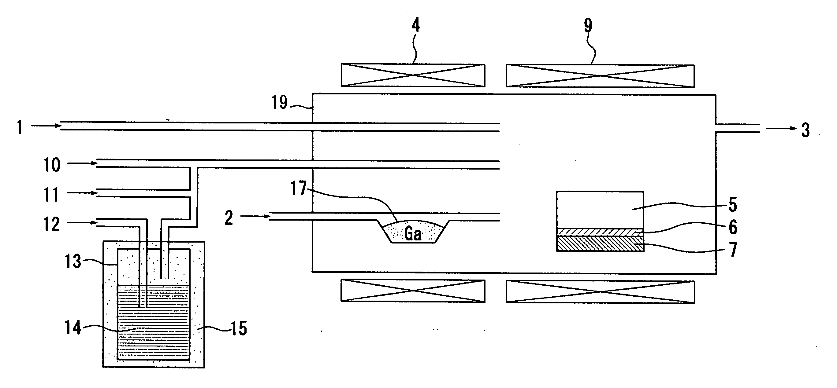
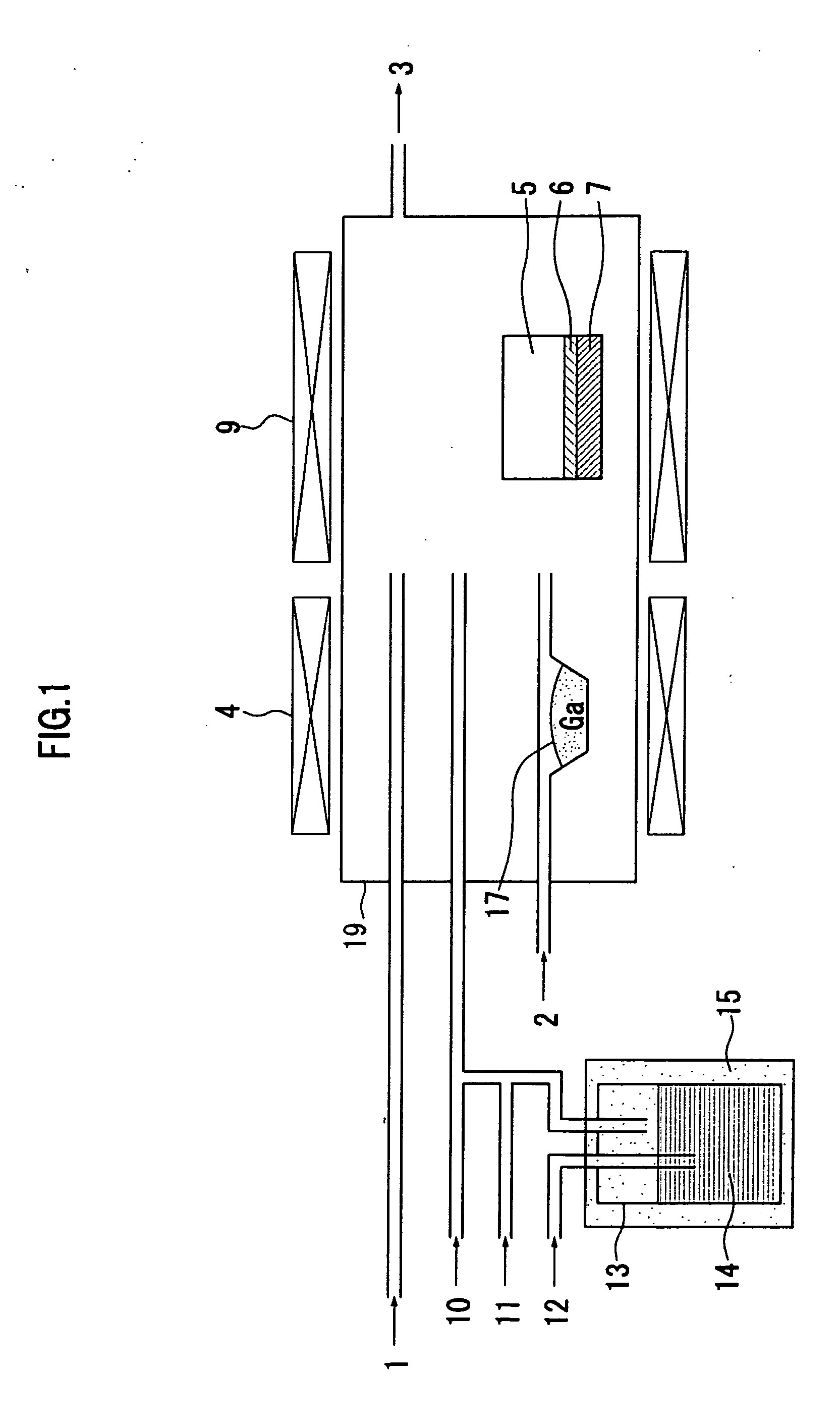
[0058]FIG. 1 shows a schematic diagram of a hot wall type HYPE apparatus to be used in a method for manufacturing a group III nitride crystal in the embodiment according to the invention.

[0059]The method for manufacturing a group III nitride crystal in the embodiment according to the invention is a method for manufacturing a group III nitride crystal by mixing a group III source material and ammonia in a reactor 19 which is made of quartz, and growing a group III nitride crystal on a support substrate 6 by a vapor phase epitaxy method, in which an organic metal containing Al as a group III source material is mixed with hydrogen halide gas, and supplied into the reactor 19, to manufacture the group III nitride crystal. The group III nitride crystal is e.g. an AlxGa1−xN (where 0<x≦1) crystal.

[0060]The group III nitride crystal preferably contains carbon for 1×101...

example 1a

[0072]A growth of a group III nitride crystal was conducted by using the HVPE apparatus shown in FIG. 1. TMA was used as the organic metal source material 14 of Al. The temperature of the constant temperature reservoir 15 was set to be 19° C. TMA was bubbled by N2 as a bubbling gas 12, and mixed with HCl gas 11. Thereafter, the mixed gas was conveyed by the carrier gas 10 to a growth region. N2 was used for the carrier gas 10 of a TMA+HCl line. A growth pressure was set to be the normal pressure.

[0073]In addition, only the carrier gas 2 (N2) was supplied onto the Ga melt 17. Here, the temperature of the source material generating unit (i.e. the temperature of the Ga melt 17) was set to be 850° C.

[0074]In the growth region, an Al source material and the ammonia gas 1 were mixed on a c-plane sapphire substrate 6 (a diameter of 2 inches) mounted on the susceptor 7 made of graphite and heated at 1100° C., so that the AlN crystal (a diameter of 2 inches) was grown on the substrate 6.

[007...

example 1b

[0079]A growth of a group III nitride crystal was conducted by using the HVPE apparatus shown in FIG. 1. TMA was used as the organic metal source material 14 of Al. The temperature of the constant temperature reservoir 15 was set to be 19° C. TMA was bubbled by N2 as a bubbling gas 12, and mixed with HCl gas 11. Thereafter, the mixed gas was conveyed by the carrier gas 10 to a growth region. N2 was used for the carrier gas 10 of a TMA+HCl line. A growth pressure was set to be the normal pressure.

[0080]Only the carrier gas 2 (N2) was supplied onto the Ga melt 17. Here, the temperature of the source material generating unit (i.e. the temperature of the Ga melt 17) was set to be 850° C.

[0081]In the growth region, an Al source material and the ammonia gas 1 were mixed on a c-plane sapphire substrate 6 (a diameter of 2 inches) mounted on the susceptor 7 made of graphite and heated at 1000° C. so that the AlN crystal (a diameter of 2 inches) was grown on the substrate 6. Herein, an NH3 pa...


PUM

PropertyMeasurementUnit
band gapaaaaaaaaaa
temperatureaaaaaaaaaa

Abstract

A method for manufacturing a group III nitride crystal includes a step of mixing a group III source material and ammonia in a reactor including quartz, and growing a group III nitride crystal on a support substrate by a vapor deposition. The group III source material is an organic metal source material containing Al. The organic metal source material is mixed with a hydrogen halide gas and the mixture of the organic metal source material and the hydrogen halide gas is supplied to the reactor.

Description

[0001]The present application is based on Japanese Patent Application No.2010-246048 filed on Nov. 2, 2010 and Japanese Patent Application No.2011-83404 filed on Apr. 5, 2011, the entire contents of which are incorporated herein by reference.BACKGROUND OF THE INVENTION[0002]1. Field of the Invention[0003]The invention relates to a method for manufacturing a group III nitride crystal, a method for manufacturing a group HI nitride template, a group III nitride crystal and a group III nitride template.[0004]2. Description of the Related Art[0005]Aluminum nitride (AlN) has an extremely wide band gap of 6.2 eV. Accordingly, by forming a mixed crystal from GaN having a band gap of 3.4 eV and AlN at an arbitrary composition ratio (AlxGa1−xN, where 0<x≦1), a crystal with a band gap of an arbitrary value between those of AlN and GaN can be obtained. Consequently, the application thereof as an ultraviolet light-emitting device or light receiving device is now under research.[0006]Since a g...

Claims


Application Information

Patent Timeline
Patent Type & Authority Applications(United States)
IPC IPC(8): C30B25/00H01B1/02H01L29/20
CPCC30B25/02C30B29/403H01L21/0262H01L21/02458H01L21/0254H01L21/0237
Inventor YOSHIDA, TAKEHIROOSHIMA, YUICHITSUCHIYA, TADAYOSHI
Owner HITACHI CABLE
Learn More