Multilayer bispectral photodiode detector

a photodiode detector and bispectral technology, applied in the field of bispectral detection, can solve the problems of affecting the quality of photodiodes, and affecting the quality of photodiodes, and achieves the effects of good temporal and spatial coherence, high packing density, and simple manufacturing

Active Publication Date: 2012-03-22
COMMISSARIAT A LENERGIE ATOMIQUE ET AUX ENERGIES ALTERNATIVES
View PDF2 Cites 4 Cited by
  • Summary
  • Abstract
  • Description
  • Claims
  • Application Information

AI Technical Summary

Benefits of technology

[0058]The object of the present invention is to propose a bispectral detector that is simple to manufacture, has good temporal and spatial coherence and a high packing density.
[0068]the form factor is smaller, thus making fabrication simpler compared with “head-to-foot” geometry according to the prior art, because it is not necessary to etch the two absorption layers, because the stack of photodiodes is of the NPNP type. the depth of the cuts is therefore reduced;

Problems solved by technology

Such detectors are bulky.
In addition, not only is adjusting the optical channels awkward, the optical channels also lose adjustment during use of the detector and this necessitates their frequent return to the manufacturer.
This geometry is more compact but the photodiodes cannot be individually addressed because, by subjecting the stack to a given potential difference, one photodiode is forward biased and the other photodiode is reverse biased.
Besides imprecise spatial coherence, detector 10 also has the disadvantage of having a non-optimal packing density.
It is therefore not possible to optimize the collection areas for each of the photodiodes.
The actual structure of detectors that have pixels with a “parallel” geometry in the example illustrated with two “planar” type diodes necessarily results in an unsatisfactory packing density and imprecise spatial coherence.
Nevertheless, “head-to-foot” geometry also poses specific problems.
It is therefore impossible to simultaneously collect the charges produced by each of the photodiodes.
This type of geometry is difficult to fabricate because of its high form factor, i.e. because cuts 64 have a high depth-to-width ratio.
Etching this type of cut and respecting the geometrical constraints, on the one hand, and avoiding introducing structural or composition defects into the materials of the islands, on the other hand, are very difficult.
Not only that, depositing passivation layer 68 over the entire surface of a cut that has a high form factor is also difficult.
“Head-to-foot” type geometry is therefore difficult to fabricate and produces detection that is not temporally coherent.

Method used


Image

  • Multilayer bispectral photodiode detector
  • Multilayer bispectral photodiode detector
  • Multilayer bispectral photodiode detector

Examples


first embodiment

[0108]A detector 60 according to a first embodiment of the invention is described below making reference to FIGS. 8 and 9. FIG. 8 is a top view showing an array of two pixels by two pixels and FIG. 9 is a cross-sectional view along line C-C in FIG. 8.

[0109]Detector 60 differs from detector 10 in FIGS. 1 to 3 by virtue of the shape of the N-type semiconductor zones implanted in layers 14 and 18 of the stack and the presence of cuts 62 around each pixel 64.

More especially, N-type zones 20 and 24 according to the prior art are, respectively, replaced by N-type layers 66 and 68 which entirely cover P-type absorption layers 14 and 18.

[0110]Advantageously, N-type layer 66 and P-type layer 14, as well as N-type layer 68 and P-type layer 18, are produced during a single epitaxial growth step by introducing appropriate dopants into the CdxHg1-xTe alloy in order to obtain the desired cadmium composition and N- or P-type properties.

[0111]The pixels are then individualized by etching cuts 62 in...

second embodiment

[0119]In the embodiment described above, the form factor of cuts 62, although considerably reduced compared with the prior art used in “head-to-foot” type detectors, may still be considered to be too high.

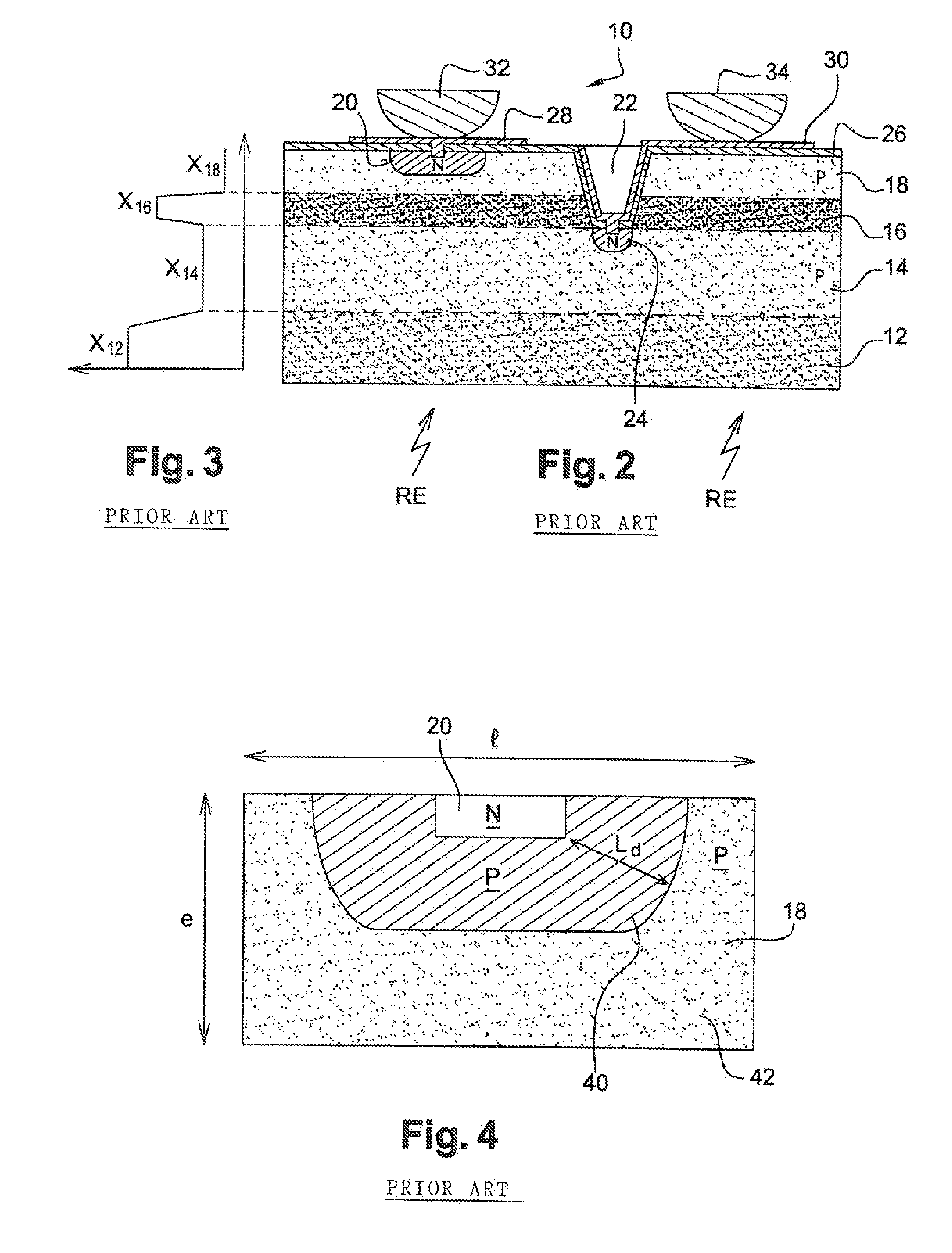
[0120]A second embodiment, illustrated by the cross-sectional view in FIG. 10, differs from the first embodiment in that the N-type semiconductor zones 24 produced in contact with absorption layer 14 in order to form the lower PN junctions are produced at the bottom of openings 22 by using a “planar” type method, in a similar way to zones 24 according to the prior art, by extrinsic doping with N-dopants, for example by ion implantation or by ion implantation and converting the P-type intrinsic doping to N-type doping or by diffusion.

[0121]Zones 24 have a diameter of 2 to 10 micrometers for example.

[0122]The upper photodiodes are then individualized by etching cuts 72 in the upper face of the assembly as far as upper absorption layer 18. The depth of cuts 72 is therefore shallow and...

third embodiment

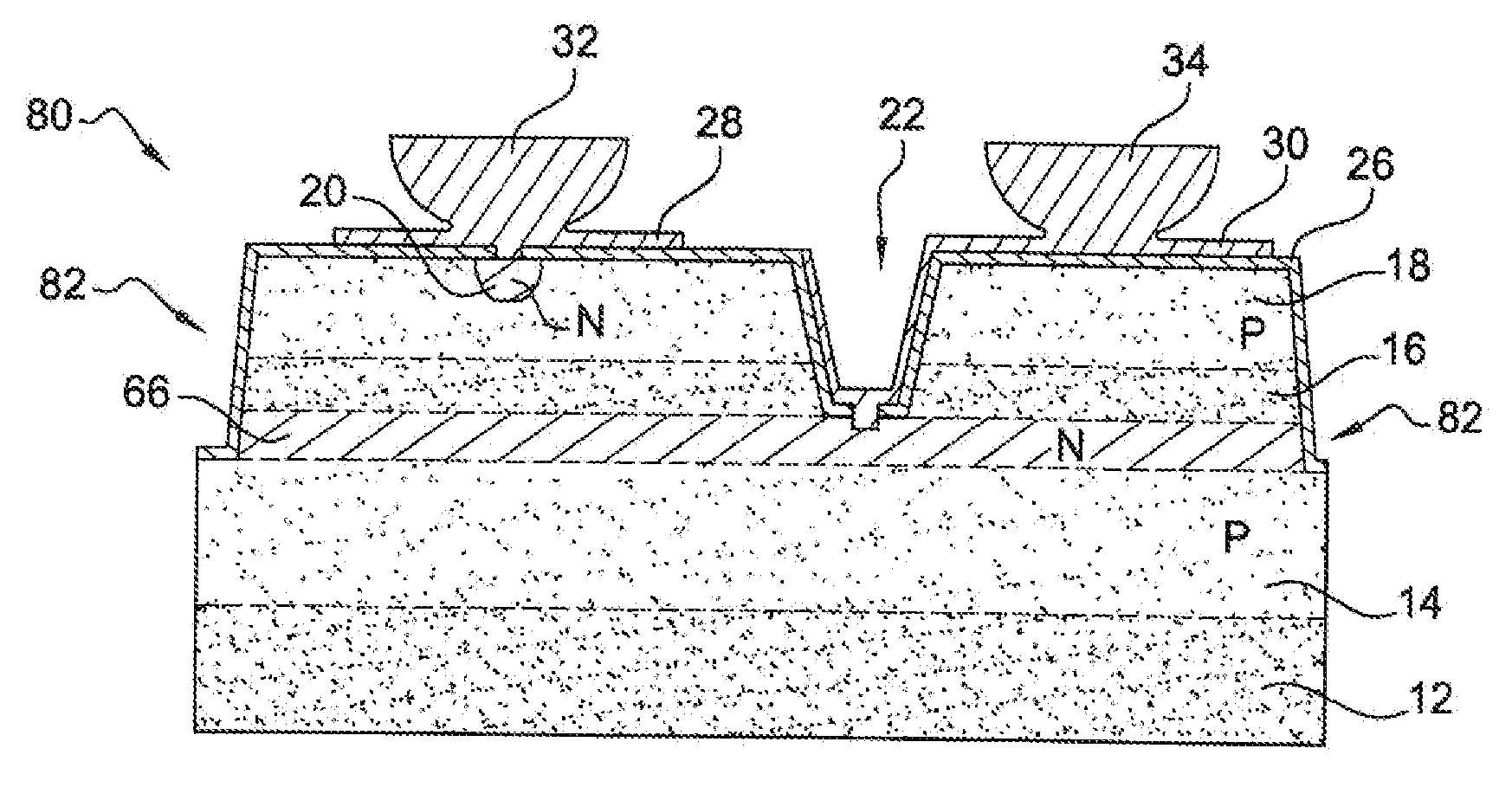
[0128]In the third embodiment, illustrated by the cross-sectional view in FIG. 11, the structure of detector 80 is inverted compared with detector 70 in the second embodiment.

[0129]More especially, the upper photodiodes are of the “planar” type with N-type semiconductor zones 20 implanted in absorption layer 18 in a similar manner to those according to the prior art. The lower photodiodes are of the “mesa” type and are formed by N-type layer 66 which covers P-type absorption layer 14, with cuts 82 being made in the upper face of the assembly as far as layer 14 in order to individualize the pixels.

[0130]Here, the packing density of lower photodiodes 66, 14 is optimal by design, bearing in mind the desired thickness for absorption layer 14, and the packing density of upper photodiodes 20, 18 is advantageously maximized by increasing the diffusion length Ld in layer 18 by applying an appropriate heat treatment such as that described, for instance, in the document entitled “Electrical d...


PUM


Abstract

This bispectral detector comprises a plurality of unitary elements for detecting a first and a second electromagnetic radiation range, consisting of a stack of upper and lower semiconductor layers of a first conductivity type which are separated by an intermediate layer that forms a potential barrier between the upper and lower layers; and for each unitary detection element, two upper and lower semiconductor zones of a second conductivity type opposite to the first conductivity type, are arranged respectively so that they are in contact with the upper faces of the upper and lower layers so as to form PN junctions, the semiconductor zone being positioned, at least partially, in the bottom of an opening that passes through the upper and intermediate layers. The upper face of at least one of the upper and lower layers is entirely covered in a semiconductor layer of the second conductivity type. Cuts are made around each unitary detection element from the upper face of the stack and at least through the thickness of each semiconductor layer of the second conductivity type, entirely covering one or other of the upper and lower semiconductor layers of the first conductivity type, so as to form semiconductor zones of the second conductivity type.

Description

CROSS REFERENCE TO RELATED APPLICATION[0001]This application claims benefit of French Patent Application No. 1057392, filed on Sep. 16, 2010. The entirety of this application is incorporated herein by reference.FIELD OF THE INVENTION[0002]The invention relates to the field of bispectral detection and, more especially, bispectral detection using unitary detection elements consisting of a stack of different absorption layers.DESCRIPTION OF PRIOR ART[0003]Bispectral detection and, in particular, detection in two separate infrared ranges such as the mid infrared range (2.5-5.5 μm) and the far infrared range (8-12 μm), has many applications, especially in the field of earth observation, meteorology, etc.[0004]Ideally, the images formed by a bispectral detector in each of its two detection ranges are spatially coherent, i.e. they correspond to the same observed scene, temporally coherent, i.e. they correspond to the same detection instant, and have a high resolution, i.e. they consist of ...

Claims


Application Information

Patent Timeline
IPC IPC(8): H01L31/102H01L31/18
CPCH01L27/14641H01L27/14652Y02E10/50H01L31/11H01L31/1832H01L27/14696H01L31/1013
Inventor GRAVRAND, OLIVIERBAYLET, JACQUES
Owner COMMISSARIAT A LENERGIE ATOMIQUE ET AUX ENERGIES ALTERNATIVES
Why Eureka
Try Eureka