Method for producing metal laminated substrate for oxide superconducting wire, and oxide superconducting wire using the substrate
a technology of oxide superconducting wire and metal laminated substrate, which is applied in the direction of superconducting magnets/coils, magnetic bodies, superconductor devices, etc., can solve the problems of low material strength of crystal-oriented ni, deterioration of superconducting properties, and 30 mpa in yield stress, etc., to achieve stable crystal orientation, good elasticity, and good elasticity
- Summary
- Abstract
- Description
- Claims
- Application Information
AI Technical Summary
Benefits of technology
Problems solved by technology
Method used
Image
Examples
embodiment 1
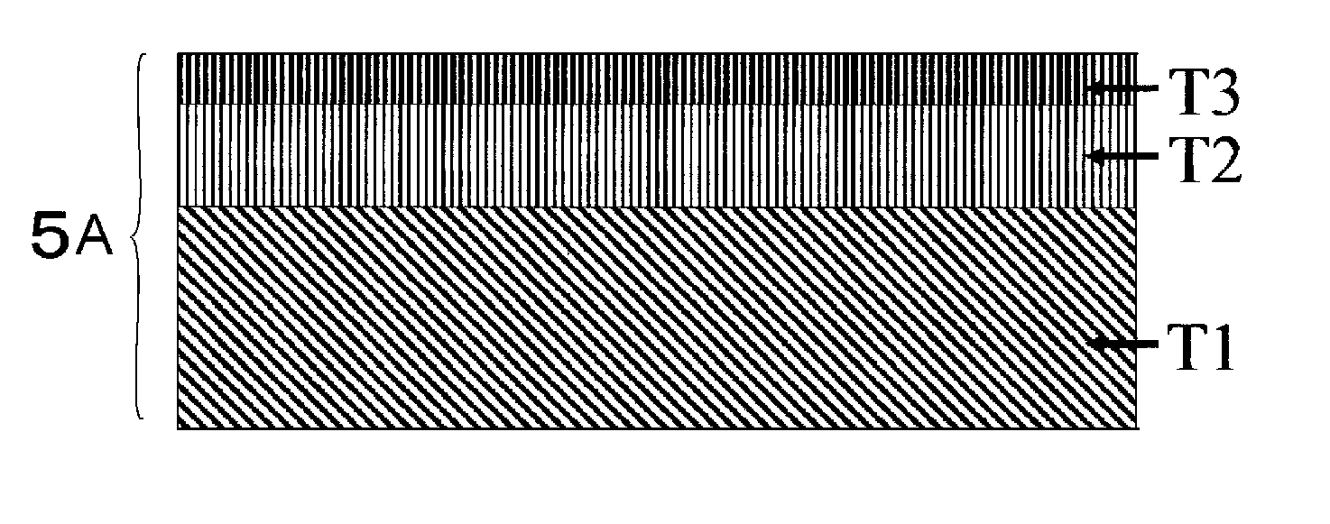
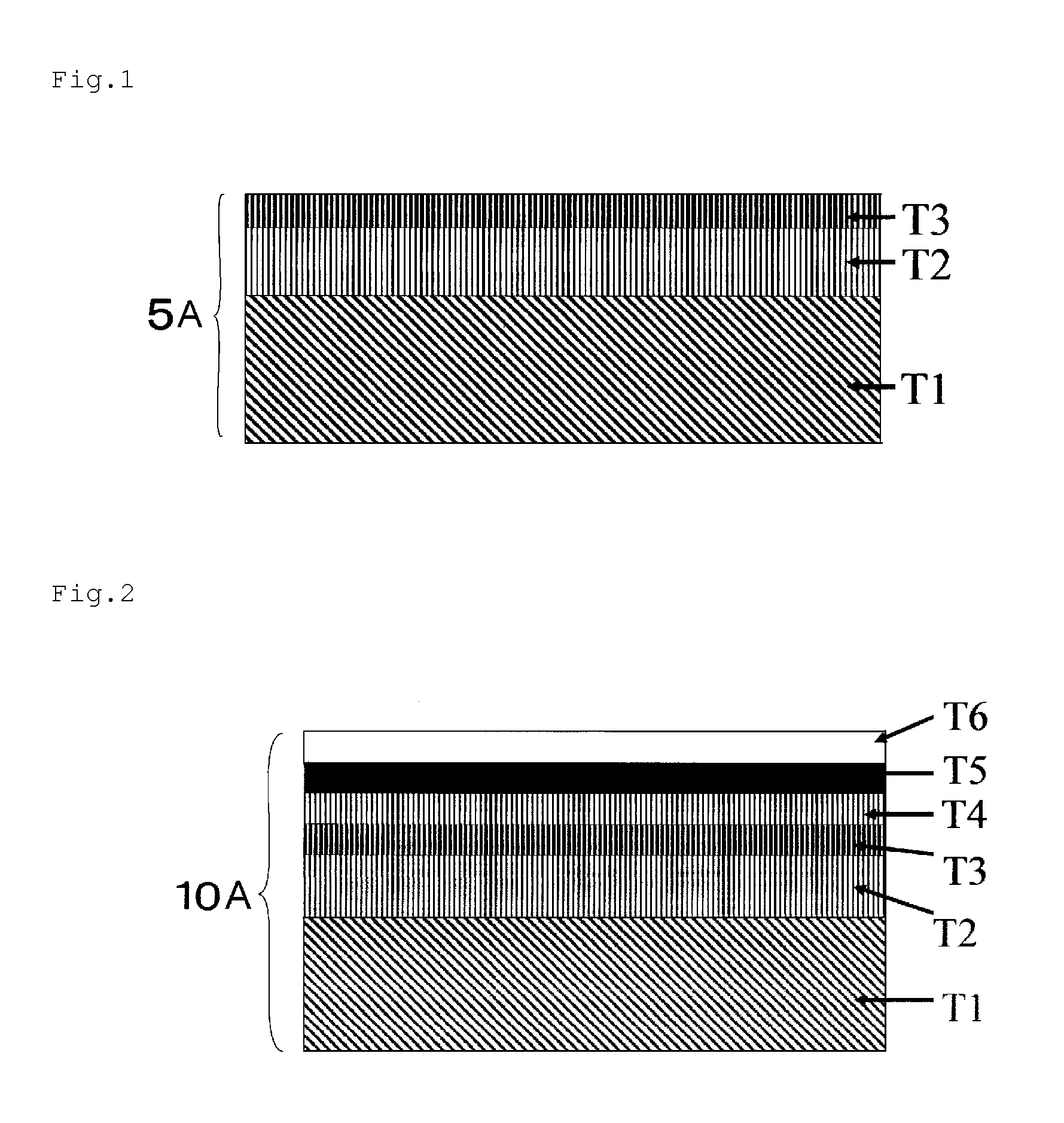
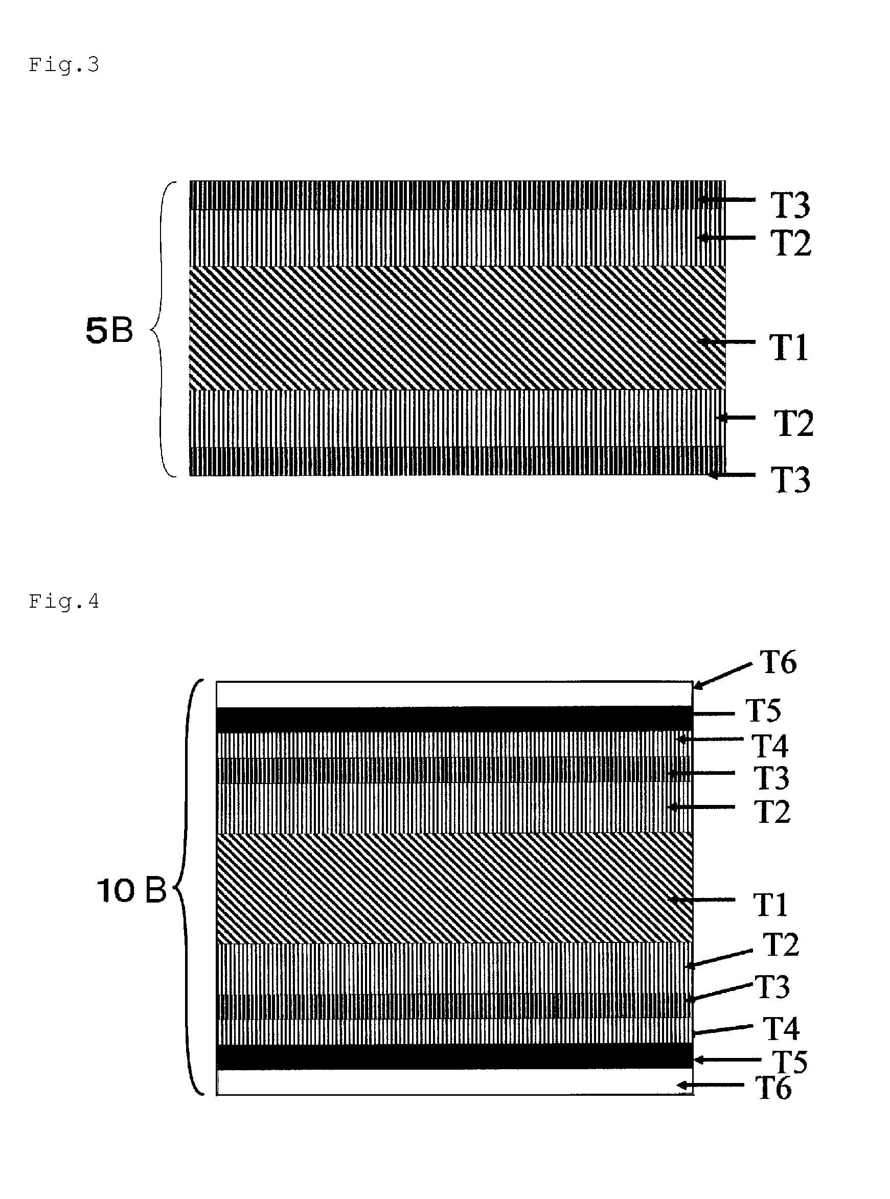
[0108]A high-reduction rolled Cu foil having a width of 200 mm and a thickness of 18 μm and a SUS316L plate having a width of 200 mm and a thickness of 100 μm are bonded to each other by a room-temperature activation bonding method, the high-reduction rolled Cu foil and the SUS316L plate are subject to heat treatment by continuous annealing at a temperature of 800° C. (a soaking holding time: 5 minutes) and, thereafter, Ni plating is applied to the Cu foil by changing a film thickness thus acquiring metal laminated substrates for an oxide superconducting wire. Then, the substrate is subject to slit working thus forming tape-shaped samples having a width of 10 mm. Crystal orientation rates of Ni plating layers of the acquired metal laminated substrates for an oxide superconducting wire are measured.
[0109]The respective measurements are performed in accordance with the above-mentioned method with proper modification. The results of the measurements are shown in Table 2.
TABLE 2CrystalE...
embodiment 2
[0114]An intermediate layer (CeO2 / YSZ / CeO2) and an oxide superconducting body layer (RE(1)Ba(2)Cu(3)O(7-δ); RE=Y, Gd, Ho or the like) having a thickness of 1.2 μm are formed on various metal laminated substrate tapes for an oxide superconducting wire manufactured by the manufacturing method of the present invention and, thereafter, an Ag protective film is formed on the oxide superconducting body layer thus completing the oxide superconducting wire.
[0115]Table 3 shows results of measurements of superconductive properties of oxide superconducting wires obtained by the embodiment 2 and having a length of 15 cm and hysteresis generated by saturated magnetization which becomes an index of an AC loss in a state where the intermediate layer is formed.
TABLE 3CrystalNiSurfacecurrentEmbodimentthick-rough-YielddensityHys-comparisonnessnessstress(MA / teresisexampleSample(μm)Ra (nm)(MPa)cm2)(J / cm3)EmbodimentNi / SUS316L0.7704801.1—2-1LaminationEmbodimentplate1.0704801.1522-2constitutionEmbodimentN...
PUM
| Property | Measurement | Unit |
|---|---|---|
| thickness | aaaaa | aaaaa |
| thickness | aaaaa | aaaaa |
| thickness | aaaaa | aaaaa |
Abstract
Description
Claims
Application Information
 - R&D
- Intellectual Property
- Life Sciences
- Materials
- Tech Scout
- Unparalleled Data Quality
- Higher Quality Content
- 60% Fewer Hallucinations
Browse by: Latest US Patents, China's latest patents, Technical Efficacy Thesaurus, Application Domain, Technology Topic, Popular Technical Reports.
© 2025 PatSnap. All rights reserved.Legal|Privacy policy|Modern Slavery Act Transparency Statement|Sitemap|About US| Contact US: help@patsnap.com


