
Circuit and System of Aggregated Area Anti-Fuse in CMOS Processes

Active Publication Date: 2012-02-16
ATTOPSEMI TECH CO LTD
View PDF3 Cites 55 Cited by
  • Summary
  • Abstract
  • Description
  • Claims
  • Application Information

AI Technical Summary

Benefits of technology

[0013]The invention pertains to an OTP device and memory that use aggregated area to enhance program yield and reliability in breaking down an oxide near junction area and yet without requiring any additional process steps or masks over standard CMOS logic processes to save costs.
[0014]The invention pertains to an OTP device and memory that used non-LDD, special implants, and alternative polarity pulses to suppress soft breakdown so that program yield can be high. Blocking LDD and creating special implants can be achieved in standard CMOS processes by simple operations on layout database without incurring any special processing or masks. Thus, no additional costs are needed for the OTP in embedded applications.

Problems solved by technology

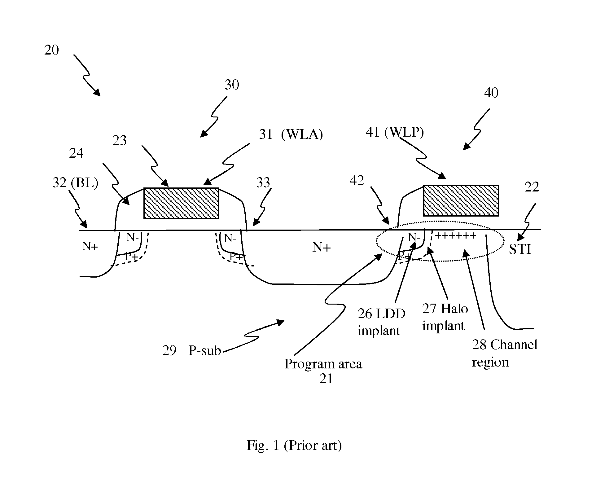
As a result, the program behavior becomes very unpredictable and the conductive current between BL and WLP varies substantially when WLA is turned on.
However, in the most cases, the gate oxide seems conductive after applying a high voltage across a thin oxide film.
But the gate oxide may become non-conductive again after cycling or burned in.
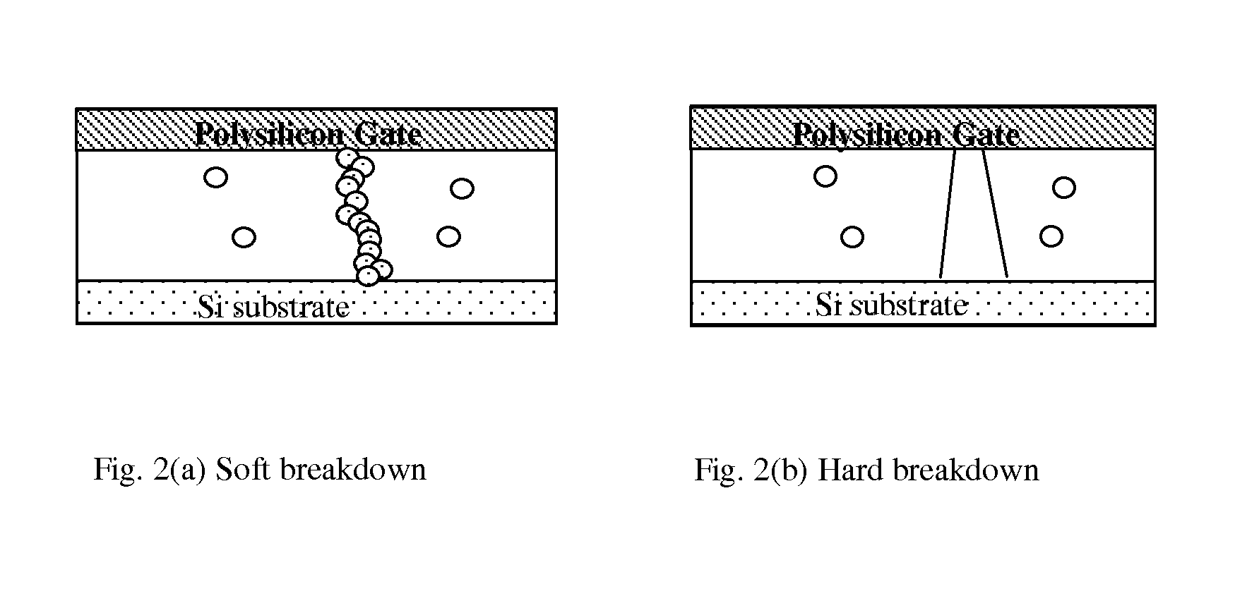
The soft breakdown effect makes the gate oxide breakdown anti-fuse very unreliable.
This mechanism becomes even worse when the gate oxide is thinner.
Besides, splitting a gate with half of thick and thin oxides can easily contaminate the delicate gate oxide and make fabrication more complicated.
As a result, the yield is not high either.

Method used


Image

  • Circuit and System of Aggregated Area Anti-Fuse in CMOS Processes
  • Circuit and System of Aggregated Area Anti-Fuse in CMOS Processes
  • Circuit and System of Aggregated Area Anti-Fuse in CMOS Processes

Examples


Embodiment Construction

[0041]This invention discloses several embodiments to increase electrical field by blocking the LDD implant, to make channel region more uniform by using special implants, and to suppress soft breakdown by applying voltages with alternative polarities. By doing so, the program yield can be increased substantially while the cell size remains small. The aggregate-area methods described above can be realized by using operations on layout database, thus no additional masks are needed over standard CMOS logic processes.

[0042]The anti-fuse cells shown in FIG. 1 and FIG. 3 have drawbacks: (1) non-uniform program area, and (2) soft breakdown issue that can easily plague the program yield and reliability. This invention discloses several embodiments to aggregate program area while suppressing soft breakdown to enhance programmability. FIG. 4 shows a cross section of an LDD device with doping concentration and electrical field profile, referred to Seiki Ogura, et al, “Design and Characteristi...


PUM

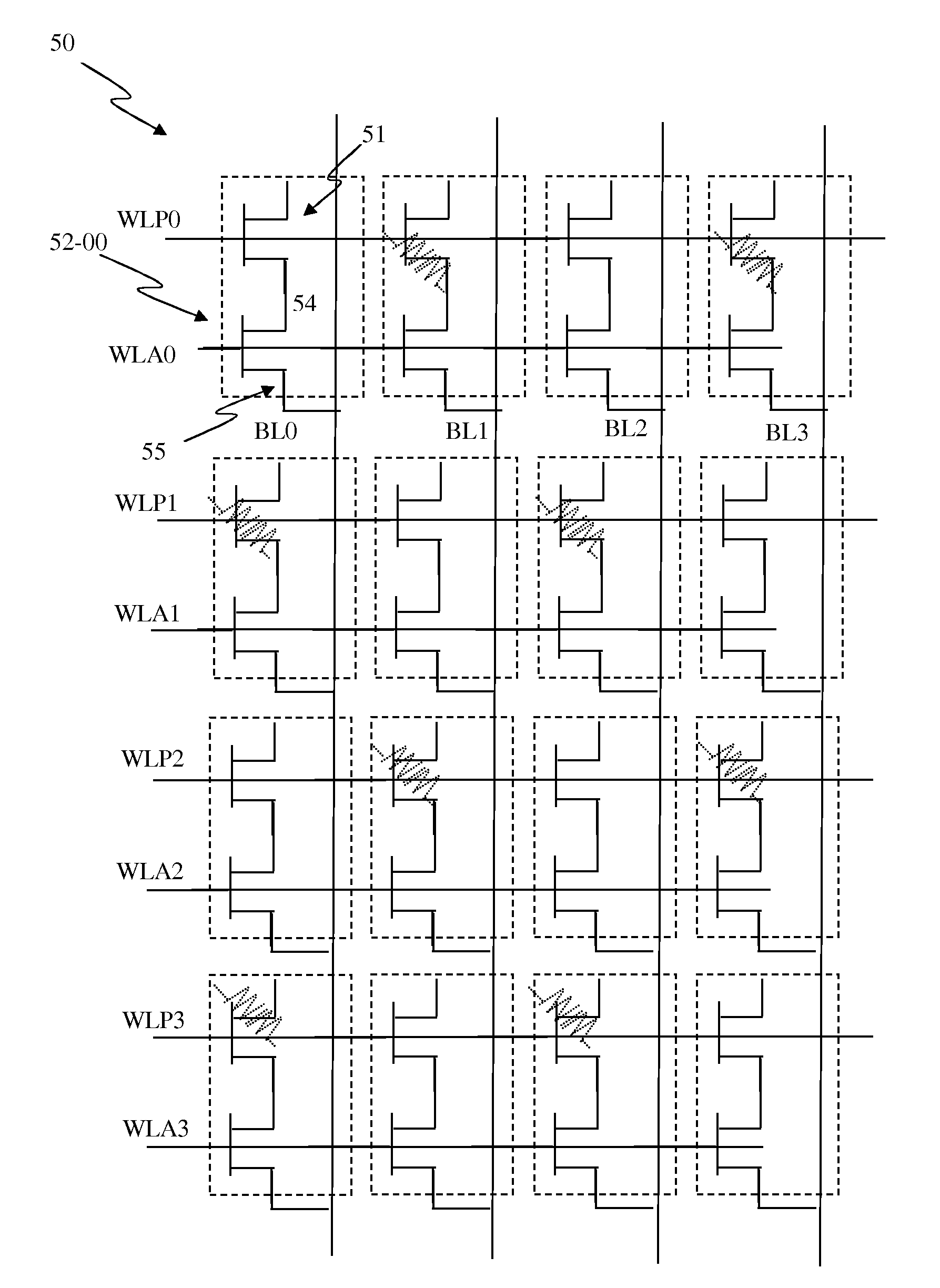

Abstract

Gate oxide breakdown anti-fuse suffers notorious soft breakdown that reduces yield and reliability. This invention discloses circuit and system to enhance electrical field by blocking LDD so that the electrical field is higher and more focused near the drain junction, to make electrical field in the channel more uniform by creating slight conductive or conductive in part or all of the channel, or to neutralize excess carriers piled up in the oxide by applying alternative polarity pulses. The embodiments can be applied in part, all, or any combinations, depending on needs. This invention can be embodied as a 2 T anti-fuse cell having an access and a program MOS with drain area in the program MOS, or 1.5 T anti-fuse cell without any drain in the program MOS. Similarly this invention can also be embodied as a 1 T anti-fuse cell having a portion of the channel made conductive or slightly conductive to merge the access and program MOS into one device with drain area, or 0.5 T anti-fuse cell without any drain.

Description

CROSS-REFERENCE TO RELATED APPLICATIONS[0001]This application claims priority benefit of U.S. Provisional Patent Application No. 61 / 372,484, filed on Aug. 11, 2010 and entitled “Circuit and System of Aggregated Area Anti-Fuse in CMOS Devices,” which is hereby incorporated herein by reference.BACKGROUND OF THE INVENTION[0002]1. Field of the Invention[0003]The present invention relates to an anti-fuse device and memories, and more particularly, to aggregate area oxide breakdown by enhancing electrical fields near the drain junction, by making channel region more uniform, or by applying alternative polarities of voltage pulses so that program area can be more restricted and programming can be more reliable.[0004]2. Description of the Related Art[0005]One-Time Programmable (OTP) devices can be programmed into a different logic state once and only once in the lifetime. OTP devices allow every integrated circuit die being customized after fabrication. They can be used for chip ID, securit...

Claims


Application Information

Patent Timeline
IPC IPC(8): G11C17/12
CPCG11C17/12H01L23/5252H01L27/0629H01L27/101H01L29/1083H01L29/7833H01L2924/0002H01L2924/00
Inventor CHUNG, SHINE C.
Owner ATTOPSEMI TECH CO LTD
Learn More