
Semiconductor laser apparatus and optical apparatus

a laser apparatus and semiconductor technology, applied in the direction of lasers, semiconductor lasers, solid-state devices, etc., can solve the problems of disadvantageous deterioration easy generation of cracks in members, and easy cracking of semiconductor laser chips, so as to reduce the concentration of organic gas or the like in the sealed space of the package, the effect of easy sealing

Inactive Publication Date: 2012-02-09
SANYO ELECTRIC CO LTD
View PDF0 Cites 311 Cited by
  • Summary
  • Abstract
  • Description
  • Claims
  • Application Information

AI Technical Summary

Benefits of technology

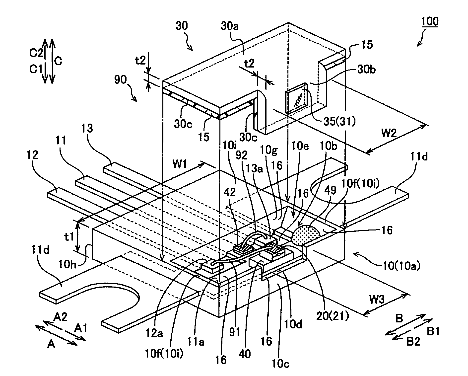
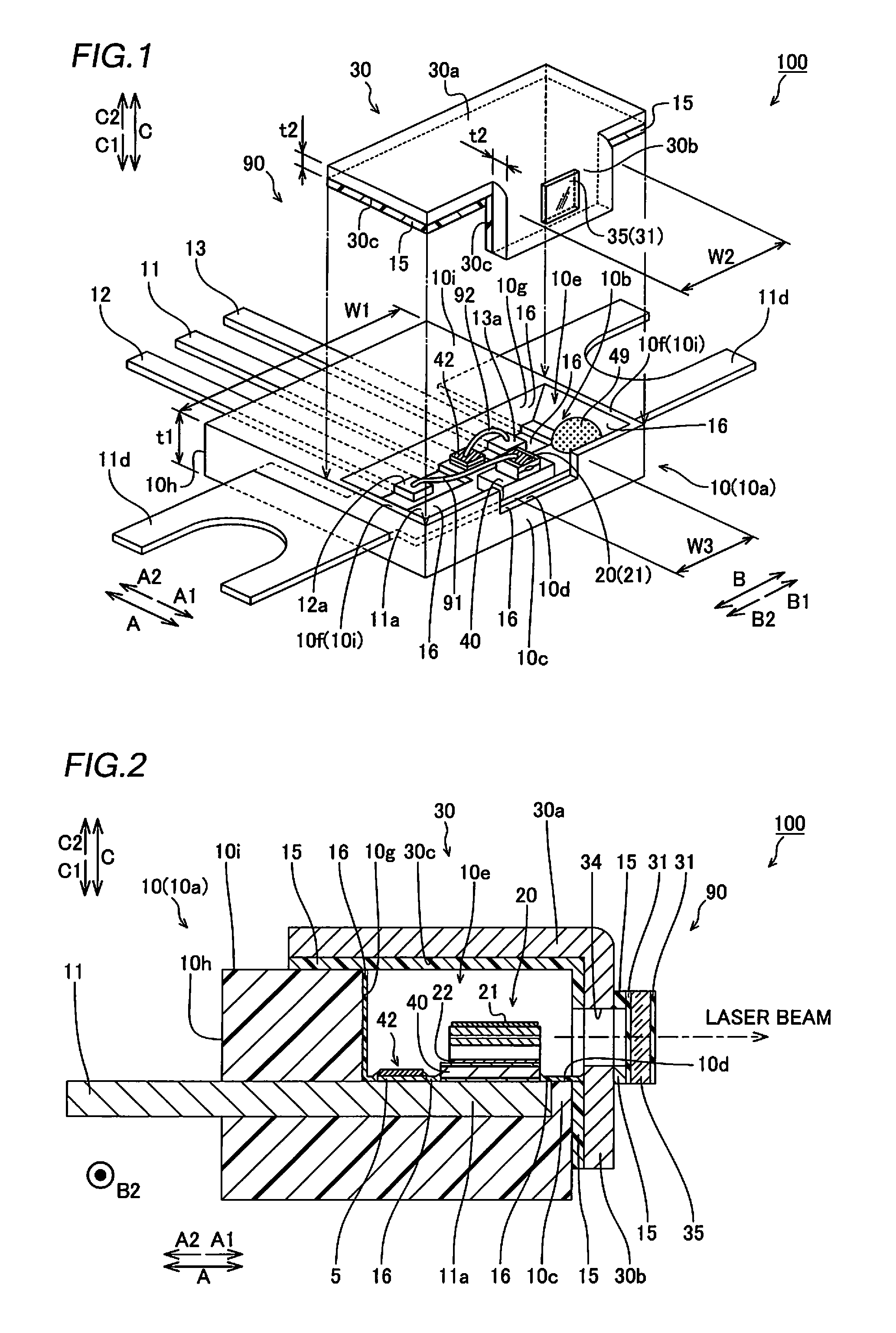
[0013]In the semiconductor laser apparatus according to the first aspect of the present invention, as hereinabove described, the surfaces of the members constituting the package located in the sealed space are covered with the covering agent made of the ethylene-polyvinyl alcohol copolymer (EVOH). The EVOH is a resin material having excellent gas barrier properties, and hence the covering agent covering the aforementioned members can block volatile organic gas from penetrating into the sealed space of the package even if the volatile organic gas is generated from the members located in the sealed space of the package. Further, even if low molecular siloxane, volatile organic gas or the like existing outside the semiconductor laser apparatus (in the atmosphere) penetrates into the components of the package, the covering agent covering the aforementioned members can inhibit the low molecular siloxane, the volatile organic gas or the like from entering the package. Further, the EVOH hardly generates the aforementioned volatile component, and hence the semiconductor laser chip in the package is not exposed to the organic gas or the like. Consequently, an adherent substance can be inhibited from being formed on a laser emitting facet, and hence the semiconductor laser chip can be inhibited from deterioration. The inventors have found as a result of a deep study that the EVOH is employed as the covering agent in the present invention.
[0031]In the aforementioned semiconductor laser apparatus according to the first aspect, the semiconductor laser chip preferably includes a nitride-based semiconductor laser chip. In the nitride-based semiconductor laser chip having a short lasing wavelength and requiring a higher output power, an adherent substance is easily formed on a laser emitting facet thereof, and hence the use of the aforementioned “covering agent” in the present invention is highly effective in inhibiting deterioration of the nitride-based semiconductor laser chip.

Problems solved by technology

Consequently, the semiconductor laser chip is disadvantageously deteriorated.
At this time, as to the EVOH resin having a thickness increased to such an extent as to form the package member, cracks are easily generated in members due to an impact from outside or the like.
Consequently, the semiconductor laser chip is disadvantageously deteriorated.

Method used


Image

  • Semiconductor laser apparatus and optical apparatus
  • Semiconductor laser apparatus and optical apparatus
  • Semiconductor laser apparatus and optical apparatus

Examples


first embodiment

Modification of First Embodiment

[0097]A semiconductor laser apparatus 105 according to a modification of the first embodiment is now described. In this semiconductor laser apparatus 105, a sealing member 30 is made of aluminum foil with a thickness of about 50 μm, as shown in FIG. 8. At this time, a sealant 15 is not applied onto an inner surface 30c of the sealing member 30 located in sealed space of a package 90, and a surface of the aluminum foil is exposed in the sealed space. On the other hand, the sealant 15 is applied with a prescribed thickness onto a peripheral region (a region near an inner wall portion 10g and respective upper surfaces of a pair of side wall portions 10f and a front wall portion 10c) of an opening 10e in an upper surface 10i of a base body 10a and a peripheral region of an opening 10d in the front surface (an outer surface (on an A1 side) of the front wall portion 10c) so as to surround the peripheries of the openings 10e and 10d shown in FIG. 1. In this ...

second embodiment

[0101]A semiconductor laser apparatus 200 according to a second embodiment of the present invention is now described. In this semiconductor laser apparatus 200, as shown in FIGS. 9 and 10, a package 90 has a base 10, and a sealing member 45 and a window member 46 both mounted on the base 10, covering a blue-violet semiconductor laser chip 20 from upper (a C2 side) and front (an A1 side) sides, respectively. While a gas absorbent 49 (see FIG. 1) is not provided in a recess portion 10b in the semiconductor laser apparatus 200, the gas absorbent 49 may be provided in the recess portion 10b.

[0102]The sealing member 45 is made of Cu alloy foil such as nickel silver with a thickness t3 of about 15 μm. The sealing member 45 has a planar shape substantially identical to a planar shape of a base body 10a, and a width W21 at the back and a width W22 at the front. A sealant 15 having a thickness of about 0.2 mm is applied onto a substantially entire region of a back surface 45c of the sealing...

third embodiment

Modification of Third Embodiment

[0131]A semiconductor laser apparatus 305 according to a modification of the third embodiment is now described. In this semiconductor laser apparatus 305, as shown in FIG. 13, a light transmission portion 35 is bonded through a sealant 15 to cover a hole 34 from the inside (inner surface 330c) of a bottom portion 330b of a cap 330. A covering agent 18 is circumferentially piled up to come into contact with the hole 34, the sealant 15 and the light transmission portion 35 in the vicinity of an inner surface of the hole 34 on which the light transmission portion 35 is mounted from inside. In other words, a side surface (inner surface) of the sealant 15 for bonding the bottom portion 330b and the light transmission portion 35 is covered with the covering agent 18. The remaining structure of the semiconductor laser apparatus 305 according to the modification of the third embodiment is substantially similar to that of the semiconductor laser apparatus 300 ...


PUM


Abstract

This semiconductor laser apparatus includes a package constituted by a plurality of members, having sealed space inside and a semiconductor laser chip arranged in the sealed space, while surfaces of the members located in the sealed space are covered with a covering agent made of an ethylene-polyvinyl alcohol copolymer.

Description

CROSS-REFERENCE TO RELATED APPLICATION[0001]The priority application number JP2010-175698, Semiconductor Laser Apparatus and Optical Apparatus, Aug. 4, 2010, Nobuhiko Hayashi et al., upon which this patent application is based is hereby incorporated by reference.BACKGROUND OF THE INVENTION[0002]1. Field of the Invention[0003]The present invention relates to a semiconductor laser apparatus and an optical apparatus, and more particularly, it relates to a semiconductor laser apparatus comprising a package sealing a semiconductor laser chip and an optical apparatus employing the same.[0004]2. Description of the Background Art[0005]A semiconductor laser device has been widely applied as a light source for an optical disc system, an optical communication system or the like in general. For example, an infrared semiconductor laser device emitting a laser beam having a wavelength of about 780 nm has been put into practice as a light source for reading of a CD, and a red semiconductor laser d...

Claims


Application Information

Patent Timeline
IPC IPC(8): H01S5/022H01S5/0232
CPCH01S5/02204H01S5/02212H01S5/02216H01S5/32341H01S5/02296H01S5/0683H01S5/02244H01L2224/48091H01L2224/48247H01S5/02235H01S5/02257H01S5/0232H01L2924/00014
Inventor HAYASHI, NOBUHIKOYOSHIKAWA, HIDEKIKURAMOTO, KEIICHIGOTO, TAKENORIOKAYAMA, YOSHIOTOKUNAGA, SEIICHI
Owner SANYO ELECTRIC CO LTD
Learn More