Semiconductor device and method of producing same
a technology of semiconductor devices and semiconductors, applied in the direction of semiconductor devices, basic electric elements, electrical equipment, etc., can solve the problems of reducing the accuracy of semiconductor devices, affecting the quality of semiconductor devices, etc., to achieve the effect of suppressing over-etching, reducing etching time, and reducing the damage to the conductive film and the first wiring layer
- Summary
- Abstract
- Description
- Claims
- Application Information
AI Technical Summary
Benefits of technology
Problems solved by technology
Method used
Image
Examples
embodiment 1
Effects of Embodiment 1
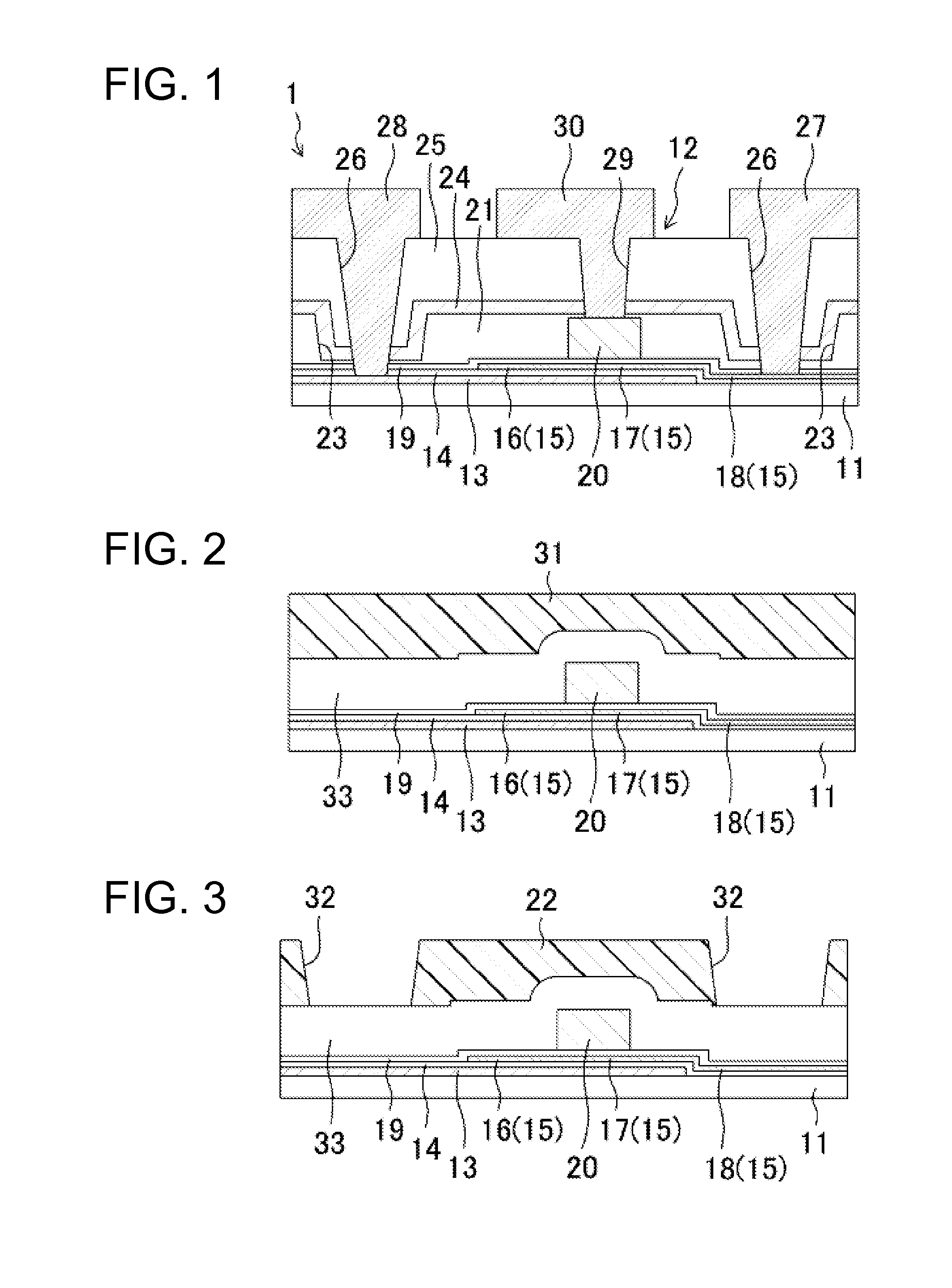
[0110]According to this Embodiment 1, because the planarizing layer 21 covering the gate electrode 20, the lower layer gate electrode 13, and the drain region 18 is made of an SiO2 film, which is an inorganic film, the semiconductor device 1 can be manufactured by a relatively high-temperature manufacturing process.
[0111]Further, because the planarizing layer 21 has the recessed portions 23 formed in the regions in which the lower layer gate electrode 13 and the drain region 18 are respectively disposed, and because the second contact holes 26 having smaller inner diameter than that of the recessed portions 23 are formed so as to run through the inside of the recessed portions 23, the aspect ratio can be reduced when the second contact holes 26 are formed.
[0112]That is, because the surface of the second interlayer insulating film 25 can be formed so as to have recesses above the recessed portions 23, the second contact holes 26 can be formed with a contact hol...
working example
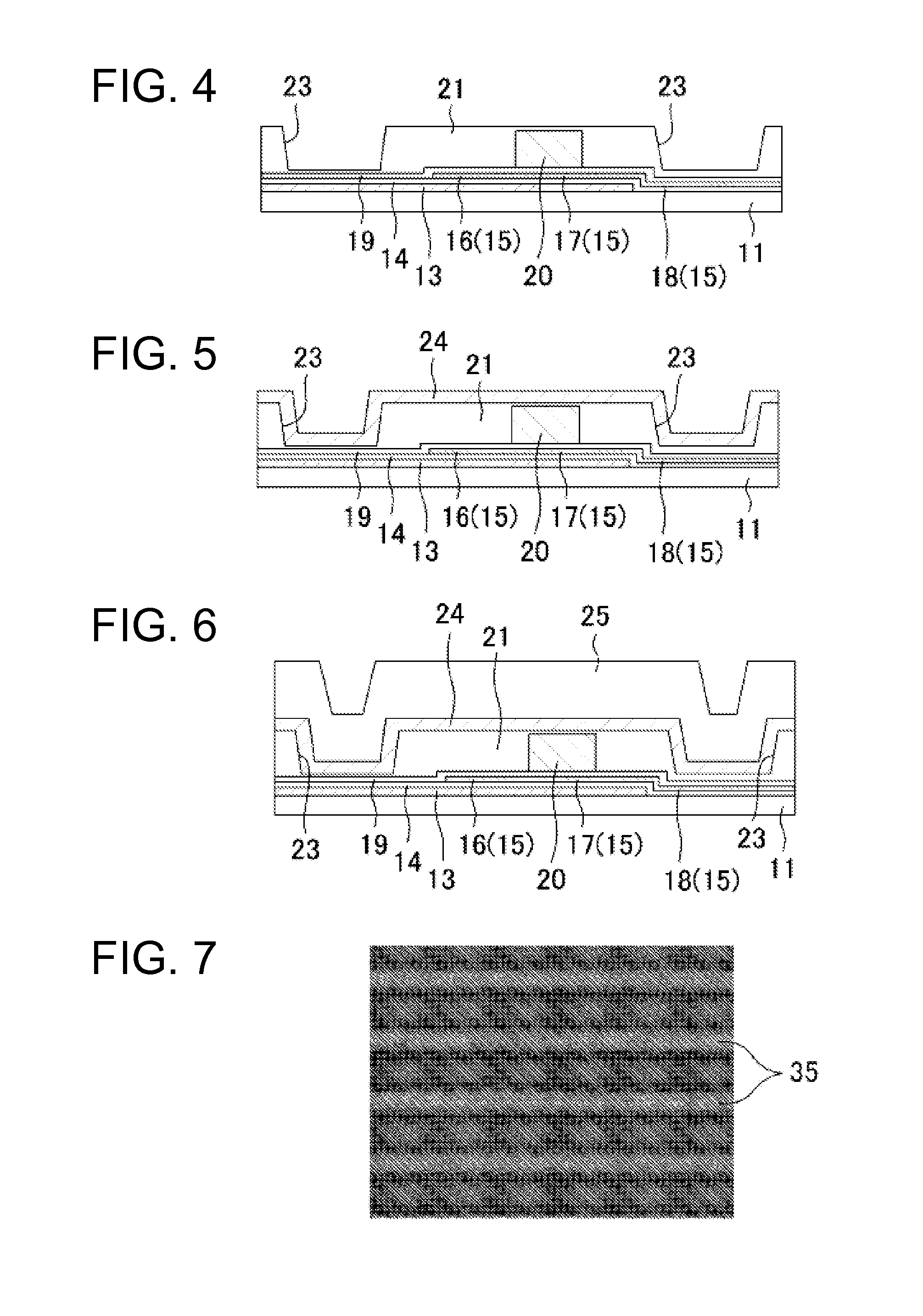
[0115]Here, FIG. 7 is a photo showing source wiring lines 35 that have been actually manufactured in a manner described above as a working example. FIG. 8 is a plan view showing a structure of the source wiring lines 35 and the gate electrodes 20. Also, FIGS. 9 to 11 are, respectively, a cross-sectional view along the line IX-IX, a cross-sectional view along the line X-X, and a cross-sectional view along the line XI-XI in FIG. 8.
[0116]FIG. 12 is a photo showing source wiring lines 135 that have been manufactured without planarization as a comparison example. FIG. 13 is a plan view showing a structure of the source wiring lines 135 and the gate electrodes 106. Also, FIGS. 14 to 16 are, respectively, a cross-sectional view along the line XIV-XIV, a cross-sectional view along the line XV-XV, and a cross-sectional view along the line XVI-XVI in FIG. 13.
[0117]In contrast to the comparison example in which the pattern of the source wiring lines 135 was formed in uneven width as shown in F...
embodiment 2
Effects of Embodiment 2
[0141]In Embodiment 2, the effects similar to those of Embodiment 1 above can also be obtained without structural problems. However, the refractive index of an SiNx film is about 2.0, and because it is higher than that of an SiO2 film, which is about 1.45, interference fringes may be generated at places depending on variations in the film thickness of the planarizing layer 21. Thus, the configuration according to Embodiment 2 is suitable for a reflective type, other than a transmissive type, liquid crystal display device, or a self-emitting type organic EL display device.
[0142]Further, because there is no first interlayer insulating film 24 and the number of film formation steps is reduced by one as compared with Embodiment 1 above, the manufacturing cost can be reduced.
Other Embodiments
[0143]In Embodiments 1 and 2 above, the semiconductor device 1 used for a liquid crystal display device has been explained. The present invention may be configured as a semicon...
PUM
 Abstract
Description
Claims
Application Information
 - R&D
- Intellectual Property
- Life Sciences
- Materials
- Tech Scout
- Unparalleled Data Quality
- Higher Quality Content
- 60% Fewer Hallucinations
Browse by: Latest US Patents, China's latest patents, Technical Efficacy Thesaurus, Application Domain, Technology Topic, Popular Technical Reports.
© 2025 PatSnap. All rights reserved.Legal|Privacy policy|Modern Slavery Act Transparency Statement|Sitemap|About US| Contact US: help@patsnap.com


