
System and Method for Manufacturing Three Dimensional Integrated Circuits

a technology of integrated circuits and manufacturing methods, applied in photomechanical treatment, printing, instruments, etc., can solve the problems of cd control of tft over more than two meters per side of g8 substrate, which is more difficult than controlling, and completely different from the manufacturing perspectiv

Active Publication Date: 2012-02-02
APPLIED MATERIALS INC
View PDF27 Cites 46 Cited by
  • Summary
  • Abstract
  • Description
  • Claims
  • Application Information

AI Technical Summary

Benefits of technology

[0029]In yet another embodiment, a method for performing automatic optical inspection includes providing an imaging writer system having a plurality of spatial light modulator (SLM) imaging units arranged in one or more parallel arrays, providing one or more patterned substrates for inspection, partitioning the one or more patterned substrates to a plurality of regions, receiving reference mask data corresponding to the one or more patterned substrates, processing the reference mask data to form a plurality of partitioned mask data patterns corresponding to the plurality of regions of the one or more patterned substrates, capturing information of the plurality of regions of the one or more patterned substrates using the plurality of SLM imaging units, analyzing information of the plurality of regions with respect to the corresponding plurality of partitioned mask data patterns to generate inspection results, and storing the inspection results in a memory device.
[0030]The method of analyzing information of the plurality of regions includes inspecting for discrepancies between the plurality of regions of the one or more patterned substrates and the corresponding plurality of partitioned mask data patterns, and identifying one or more regions of the one or more patterned substrates for repair in response to the discrepancies found in the one or more regions of the one or more patterned substrates. The method of inspecting for discrepancies includes at least one of
[0031]The method of inspecting for discrepancies includes at least one of inspecting for substrate pattern distortions between the plurality of regions of the one or more patterned substrates and the corresponding plurality of partitioned mask data patterns, and identifying one or more regions of the one or more patterned substrates for repair in response to the substrate pattern distortions found in the one or more regions of the one or more patterned substrates; inspecting for unwanted extra circuit elements on substrates of the plurality of regions of the one or more patterned substrates, and identifying one or more regions of the one or more patterned substrates for repair in response to the unwanted extra circuit elements found in the one or more regions of the one or more patterned substrates; inspecting for missing circuit elements on substrates of the plurality of regions of the one or more patterned substrates, and identifying one or more regions of the one or more patterned substrates for repair in response to the missing circuit elements found in the one or more regions of the one or more patterned substrates; and inspecting for foreign particles on substrates of the plurality of regions of the one or more patterned substrates, and identifying one or more regions of the one or more patterned substrates for repair in response to the foreign particles found in the one or more regions of the one or more patterned substrates.
[0032]The method of performing automatic optical inspection further includes re-coating photoresist on substrates of the one or more regions of the one or more patterned substrates identified for repair, performing pattern reconstruction on the one or more regions of the one or more patterned substrates identified for repair, re-inspecting the one or more regions of the one or more patterned substrates identified for repair using the plurality of SLM imaging units, and updating the inspection results in accordance with information obtained from re-inspection.
[0033]The method of performing automatic optical inspection further includes re-coating photoresist on substrates of the plurality of regions of the one or more patterned substrates, performing pattern reconstruction on the plurality of regions of the one or more patterned substrates, re-inspecting the plurality of regions of the one or more patterned substrates using the plurality of SLM imaging units, and updating the inspection results in accordance with information obtained from re-inspection.

Problems solved by technology

However, they are entirely different from the manufacturing perspective.
For the IC industry, a primary challenge is small CD features can be produced on a round 300 mm wafer.
But for the FPD industry, one primary challenge is how large an entire rectangle substrate can be processed.
In one viewpoint, one of the main challenges for FPD manufacturing is to keep throughput in pace with justifiable economics for each successive generation.
The CD control for TFT over more-than-two-meters per side of G8 substrate is more challenging than controlling specifications for printing advanced IC features on a 300 mm silicon wafer.
The challenge facing the FPD industry is to build such a mask-based exposure tool cost effectively for the upcoming FPD generations while preserving acceptable lithography process window.
Unfortunately, the tighter FPD mask CD specifications required would push the already costly mask set to be even more expensive.
In some situations, making a critical level mask for the G8 FPD becomes very expensive and has long delivery lead time.
Yet another problem with the conventional approach is the defect density control for the use of larger sized masks.
Lithography processing with such a large size mask using multiple exposures, even starting with defect free mask, is prone to introduce detrimental defects.
A defect prone process impacts yield and ultimately the cost of the mask.
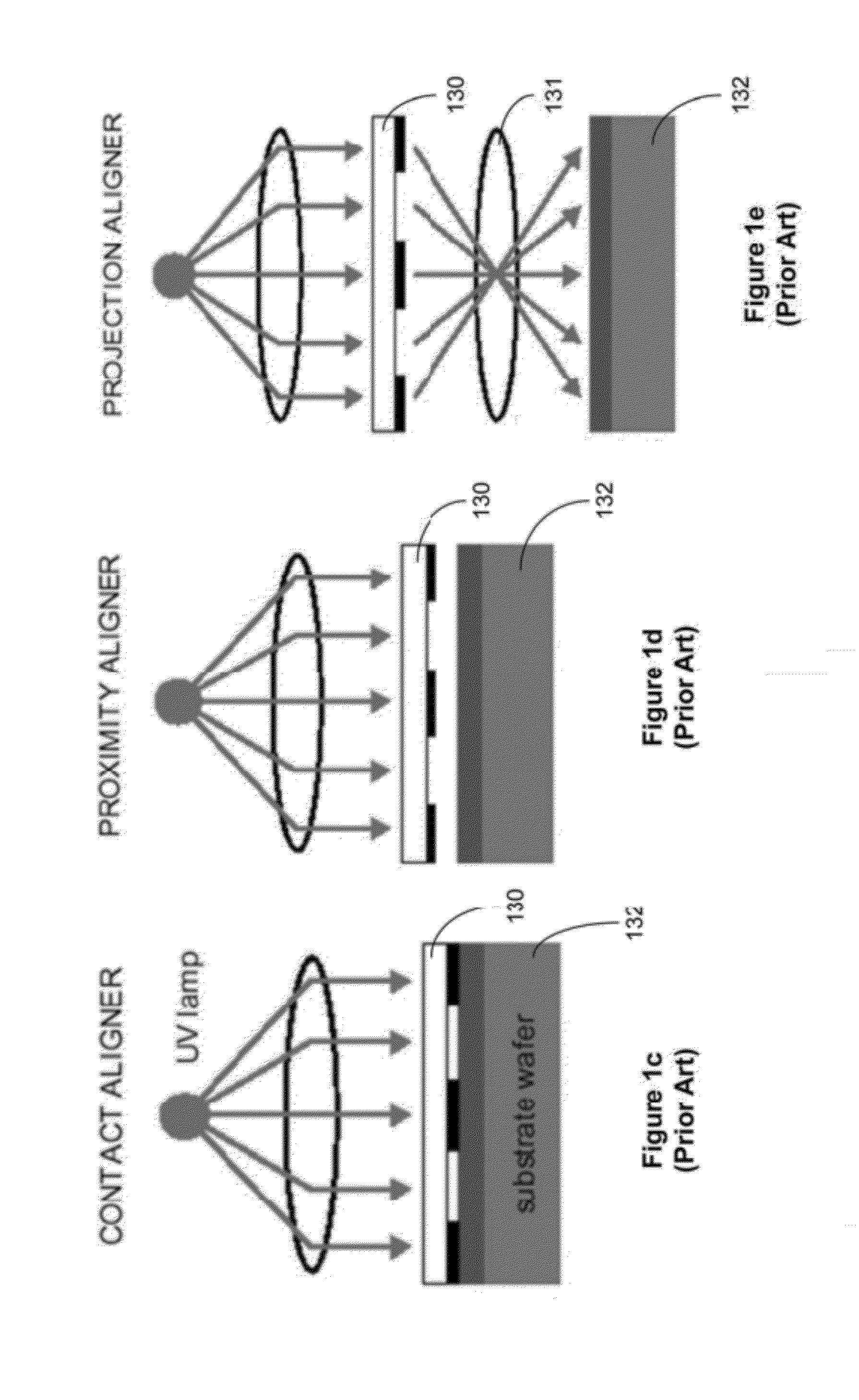
The scanner system is more efficient in handling large-sized mask flat panel displays than the stepper system, and is more expensive than the stepper system.
Some of the drawbacks of the contact aligner and proximity aligner systems are that they have problems handling high resolution designs and warped wafers or substrate larger than 4 inches in size.
The drawback is that such large-sized masks are quite expensive.
Therefore, the projection aligner system is not cost efficient for manufacturing of printed circuit boards, and light emitting diodes where substantial mask cost is less tolerable.
This writing field size is very small and therefore slow when attempting to write a full G8 FPD mask.
Such a long write time makes machine control expensive to sustain both mechanically and electronically, hence increases the cost of the FPD mask produced.
Using the same exposure tool for the upcoming G10 or beyond, the cost of manufacturing FPD masks will be even higher.
This saves the mask cost.
Unfortunately, the SLM mask has lower image quality as compared to the image quality on an actual mask.
It does not meet the pattern specification requirements for FPD manufacturing.
However, in both conventional methods described above, the mask is limited to a predetermined physical size, and the physical mask dimension essentially limits the dimension of the flexible display that can be manufactured.
Another problem with the conventional methods described by the 779 patent and the Ahn article is that, to achieve a reasonable printing result, the roll of substrate must be stretched flat during the exposure stage.
As a result, the surface flatness of the substrate is not as good as rigid glass substrate, typically used for LCD TV display.
With such a mask-based lithography, the depth of focus (DOF) is limited due to uneven substrate surface.
Thus, it can be very challenging for these conventional methods to pattern TFT feature critical dimension (CD) at 5 μm or less.
The size of the mask is too large to be manufactured cost effectively.

Method used


Image

  • System and Method for Manufacturing Three Dimensional Integrated Circuits
  • System and Method for Manufacturing Three Dimensional Integrated Circuits
  • System and Method for Manufacturing Three Dimensional Integrated Circuits

Examples


Embodiment Construction

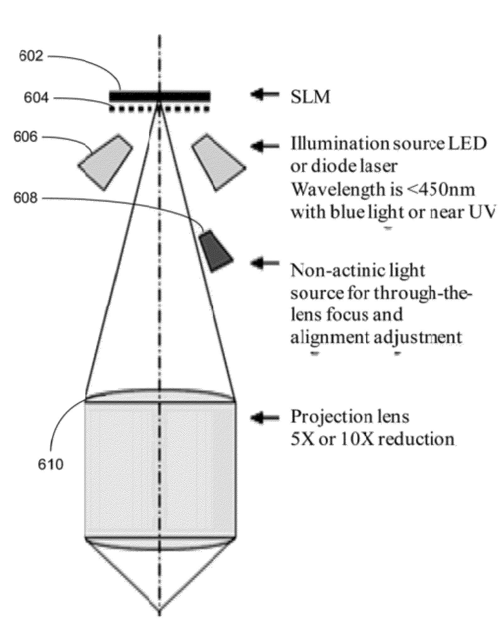
[0070]System and method are provided for manufacturing 3-D integrated circuits. The following descriptions are presented to enable any person skilled in the art to make and use the invention. Descriptions of specific embodiments and applications are provided only as examples. Various modifications and combinations of the examples described herein will be readily apparent to those skilled in the art, and the general principles defined herein may be applied to other examples and applications without departing from the spirit and scope of the invention. Thus, the present invention is not intended to be limited to the examples described and shown, but is to be accorded the widest scope consistent with the principles and features disclosed herein.

[0071]Some portions of the detailed description that follows are presented in terms of flowcharts, logic blocks, and other symbolic representations of operations on information that can be performed on a computer system. A procedure, computer-ex...


PUM


Abstract

System and method for manufacturing three-dimensional integrated circuits are disclosed. In one embodiment, the method includes providing an imaging writer system that includes a plurality of spatial light modulator (SLM) imaging units arranged in one or more parallel arrays, receiving mask data to be written to one or more layers of the three-dimensional integrated circuit, processing the mask data to form a plurality of partitioned mask data patterns corresponding to the one or more layers of the three-dimensional integrated circuit, assigning one or more SLM imaging units to handle each of the partitioned mask data pattern, and controlling the plurality of SLM imaging units to write the plurality of partitioned mask data patterns to the one or more layers of the three-dimensional integrated circuits in parallel. The method of assigning performs at least one of scaling, alignment, inter-ocular displacement, rotational factor, or substrate deformation correction.

Description

CROSS REFERENCE TO RELATED APPLICATIONS[0001]This application is a continuation-in-part of, and claims priority under 35 U.S.C. §120 to United States non-provisional patent application bearing Ser. No. 12 / 475,114, filed May 29, 2009, which claims the benefit of U.S. non-provisional application Ser. No. 12 / 337,504, filed Dec. 17, 2008, which claims the benefit of U.S. provisional application No. 61 / 099,495, “An Optical Imaging Writer System” filed Sep. 23, 2008. This application also claims the benefit of U.S. provisional application No. 61 / 379,732, “System and Method for Manufacturing Three Dimensional Integrated Circuits” filed Sep. 3, 2010. The aforementioned United States applications are hereby incorporated by reference in their entirety.FIELD OF THE INVENTION[0002]The present invention relates to the field of integrated circuit manufacturing. In particular, the present invention relates to system and method for manufacturing three dimensional (3-D) integrated circuits.BACKGROUN...

Claims


Application Information

Patent Timeline
Patent Type & Authority Applications(United States)
IPC IPC(8): G03B27/42
CPCG03F7/70275G03F7/70283G03F7/70291G03F7/70391G03F7/70475G03F7/70433G03F7/70491G03F7/70508G03B27/42
Inventor CHEN, JANG FUNGLAIDIG, THOMAS
Owner APPLIED MATERIALS INC
Learn More