Liquid crystal display panel

a liquid crystal display panel and liquid crystal technology, applied in optics, non-linear optics, instruments, etc., can solve the problems of poor insufficient anchoring energy of the alignment surface, and insufficient liquid crystal efficiency of the lcd panel. achieve good liquid crystal efficiency (transmittance

Inactive Publication Date: 2012-01-05
AU OPTRONICS CORP
View PDF6 Cites 4 Cited by
  • Summary
  • Abstract
  • Description
  • Claims
  • Application Information

AI Technical Summary

Benefits of technology

[0009]The invention is directed to a liquid crystal display (LCD) panel having good liquid crystal efficiency (transmittance).

Problems solved by technology

Although the non-contact alignment process can resolve problems of static electricity and particle pollution, etc. occurred in the contact alignment process, a problem of inadequate anchoring energy of an alignment surface is generally occurred.
If the anchoring energy of the alignment surface is inadequate, the LCD panel probably have a poor display quality.
However, when the cell gap of the LCD panel is reduced, the liquid crystal efficiency of the LCD panel is accordingly reduced.
For example, when the cell gap of the PSA LCD panel is reduced, due to twist in azimuthal angle of the liquid crystal molecules, dark lines (disclination) may occurred on an area corresponding to the alignment slit, and the dark lines (disclination) may lead to deterioration of transmittance of the LCD panel.
Therefore, how to simultaneously increase the response speed and the transmittance of the LCD panel is an important issue.

Method used


Image

  • Liquid crystal display panel
  • Liquid crystal display panel
  • Liquid crystal display panel

Examples


Embodiment Construction

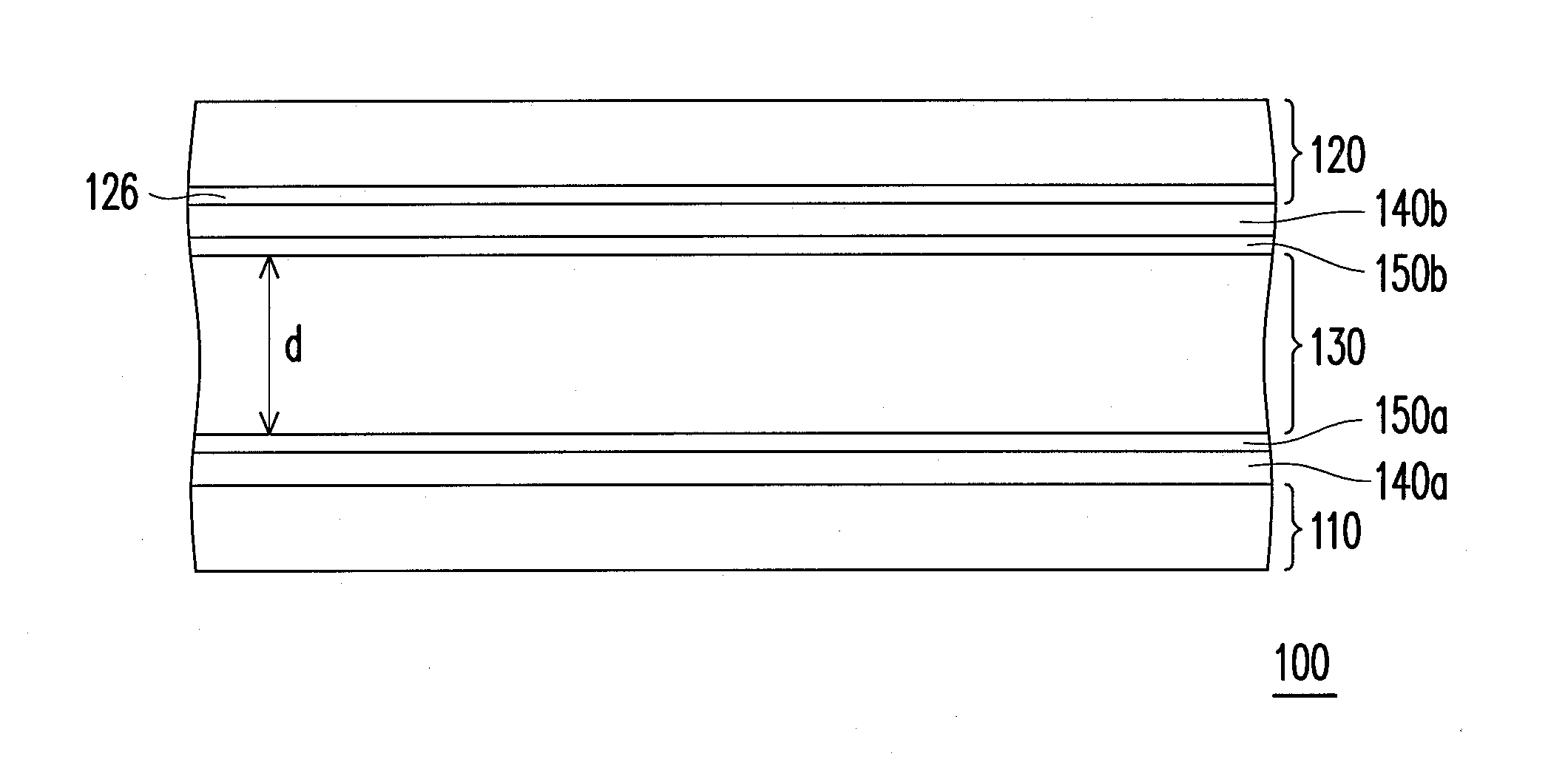
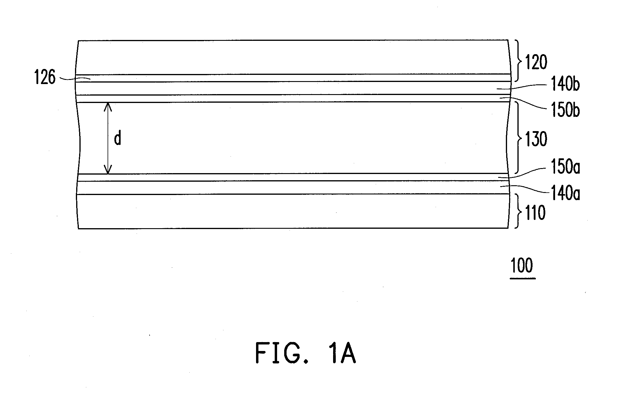
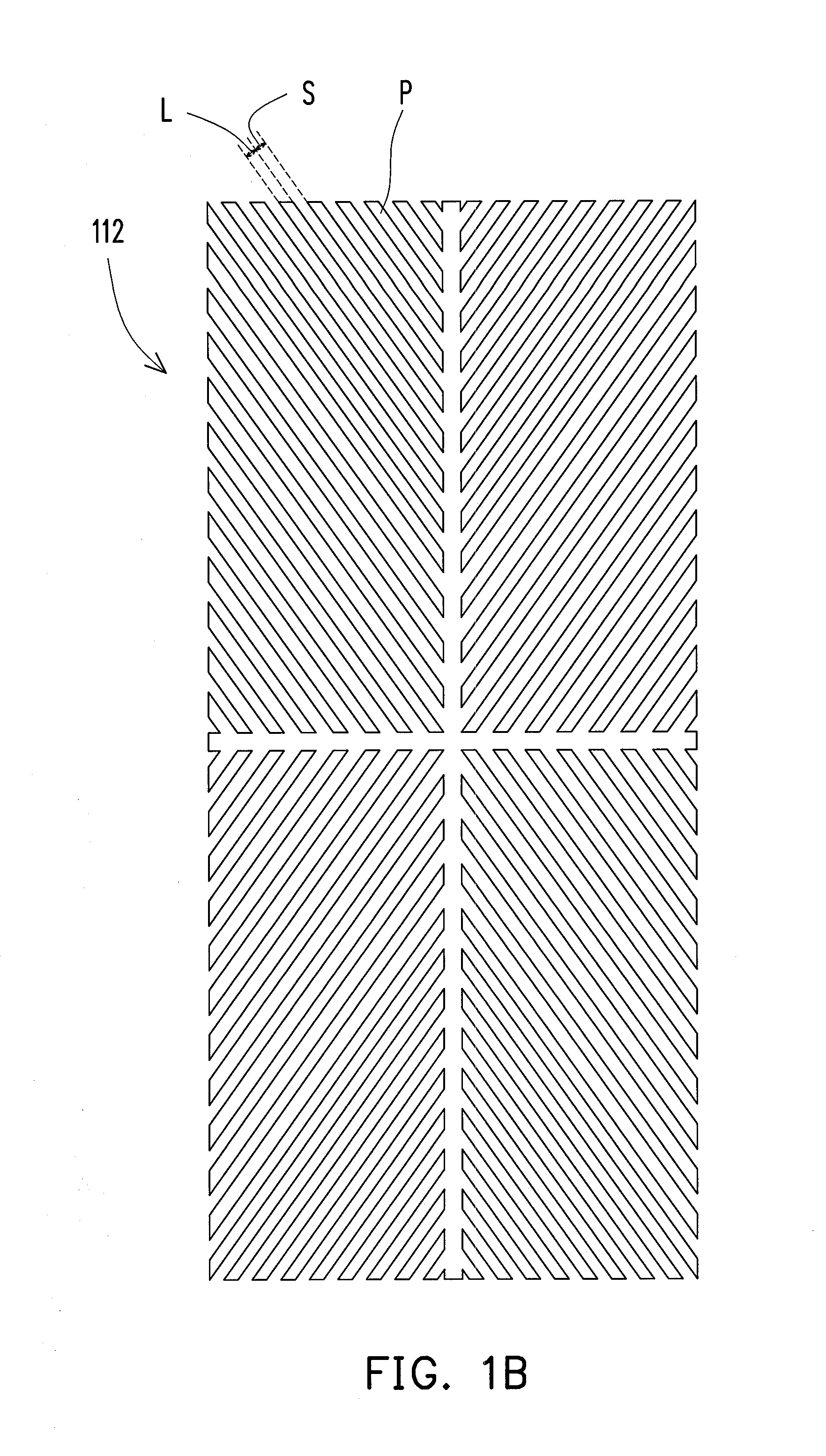
[0027]FIG. 1A is a cross-sectional view of a polymer stabilized alignment (PSA) liquid crystal display (LCD) panel according to an embodiment of the invention, and FIG. 1B is a schematic diagram of a pixel electrode according to an embodiment of the invention. Referring to FIG. 1A and FIG. 1B, the PSA LCD panel 100 of the present embodiment includes an active device array substrate 110, an opposite substrate 120, and a liquid crystal layer 130. The active device array substrate 110 includes a plurality of pixel electrodes 112, and each of the pixel electrodes 112 includes a plurality of sets of stripe patterns P extending along different directions. Each of the stripe patterns P has a width of L, and a space between two neighboring stripe patterns P is S. The opposite substrate 120 is disposed over the active device array substrate 110. The liquid crystal layer 130 is disposed between the active device array substrate 110 and the opposite substrate 120. A cell gap between the active...


PUM

PropertyMeasurementUnit
widthaaaaaaaaaa
birefringenceaaaaaaaaaa
dielectric anisotropyaaaaaaaaaa

Abstract

A liquid crystal display panel including an active device array substrate, an opposite substrate, and a liquid crystal layer is provided. The active device array substrate includes a plurality of pixel electrodes and each of the pixel electrodes includes a plurality of sets of stripe patterns extending along different directions. Each of the stripe patterns has a width of L and a space between two neighboring stripe patterns is S. The opposite substrate is disposed over the active device array substrate. The liquid crystal layer is disposed between the active device array substrate and the opposite substrate. A cell gap between the active device array substrate and the opposite substrate is d, birefringence of the liquid crystal layer is Δn, and dielectric anisotropy of the liquid crystal layer is Δ∈, wherein S, d, Δn, and Δ∈ comply with the inequality: S/|Δ∈|≦2.8×Δn×d.

Description

CROSS-REFERENCE TO RELATED APPLICATION[0001]This application claims the priority benefit of Taiwan application serial no. 99121480, filed on Jun. 30, 2010. The entirety the above-mentioned patent application is hereby incorporated by reference herein and made a part of specification.BACKGROUND[0002]1. Field of the Invention[0003]The invention relates to a liquid crystal display panel. More particularly, the invention relates to a polymer stabilized alignment (PSA) liquid crystal display panel.[0004]2. Description of Related Art[0005]In development of display technology, with progress of photoelectric technology and semiconductor manufacturing technology, liquid crystal displays (LCDs) having advantages of high image quality, good space utilization efficiency, low power consumption, and no irradiation, etc. become popular in the market.[0006]During a fabrication process of an LCD panel, alignment films are formed on two substrates, so that the liquid crystal molecules may have specif...

Claims


Application Information

Patent Timeline
Patent Type & Authority Applications(United States)
IPC IPC(8): G02F1/1335
CPCG02F1/133707G02F2001/13775G02F1/133711G02F1/13775
Inventor PAI, CHIA-HSUANCHEN, TE-SHENGCHAN, TE-WEIHSU, WEN-HAOLIN, HSI-CHIENTSAI, SHIH-CHICHIU, CHUNG-YI
Owner AU OPTRONICS CORP
Why Eureka
Try Eureka