Liquid crystal panels

a liquid crystal panel and liquid crystal technology, applied in non-linear optics, instruments, optics, etc., can solve the problems of inability to achieve small-sized, high-resolution panels, etc., to enhance the liquid crystal efficiency of va modes, enhance the alignment of liquid crystal correspondings, and reduce the width of dark lines caused by primary electrodes.

Inactive Publication Date: 2016-09-29
SHENZHEN CHINA STAR OPTOELECTRONICS TECH CO LTD
View PDF5 Cites 4 Cited by
  • Summary
  • Abstract
  • Description
  • Claims
  • Application Information

AI Technical Summary

Benefits of technology

[0020]In view of the above, the surface of the second substrate contacting with the liquid crystal panel has recessed portions formed thereon, and each of the recessed portions faces toward one corresponding primary electrode of the pixel electrode. An electrical field is formed at the recessed portions so as to enhance the alignment of the liquid crystal corresponding to the recessed portions. In this way, the width of the dark lines caused by the primary electrode is decreased so as to enhance the liquid crystal efficiency of the pixels of VA modes, and the applicable range of ultra-high-resolution, small-sized panels of VA mode is extended.

Problems solved by technology

However, the width of the dark lines caused by the electrodes of the liquid crystal panel may still affect the liquid crystal efficiency such that it is not feasible for the small-sized, high resolution panels to adopt the liquid crystal panels.

Method used


Image

  • Liquid crystal panels
  • Liquid crystal panels
  • Liquid crystal panels

Examples


Embodiment Construction

[0034]Embodiments of the invention will now be described more fully hereinafter with reference to the accompanying drawings, in which embodiments of the invention are shown.

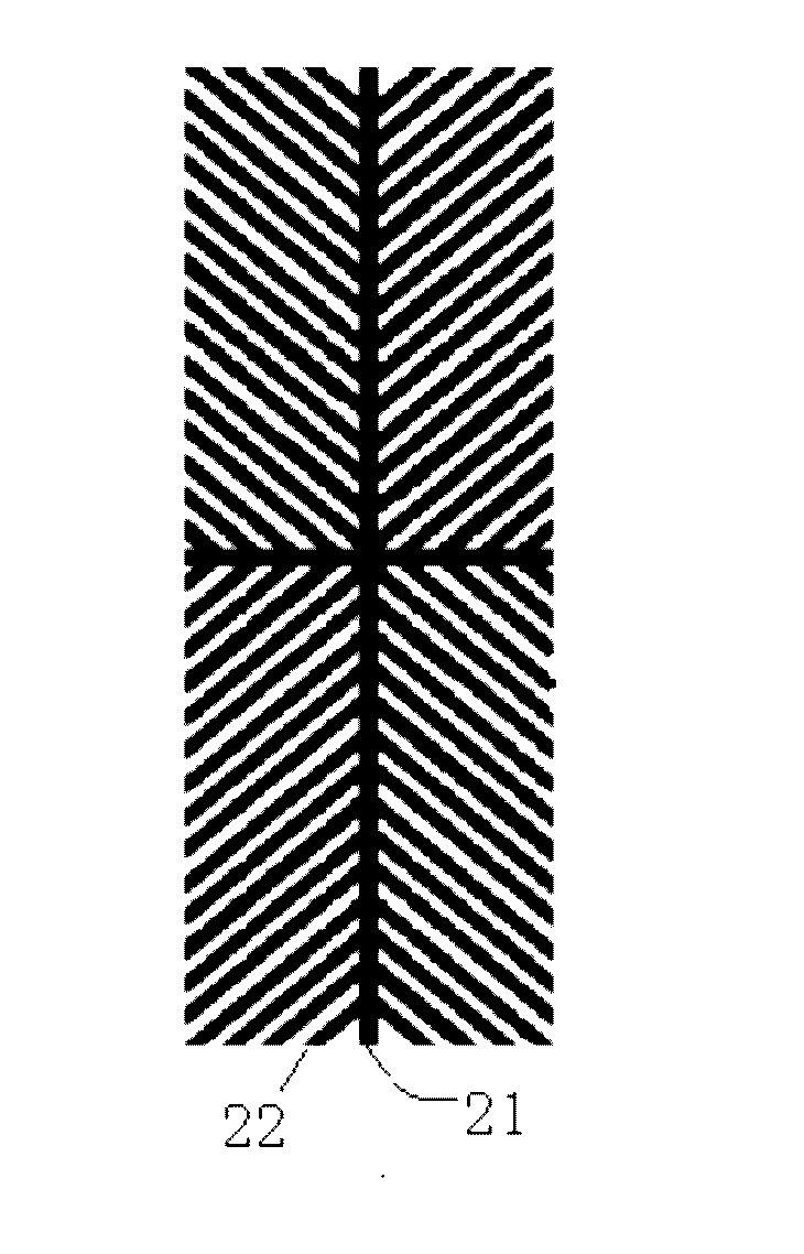
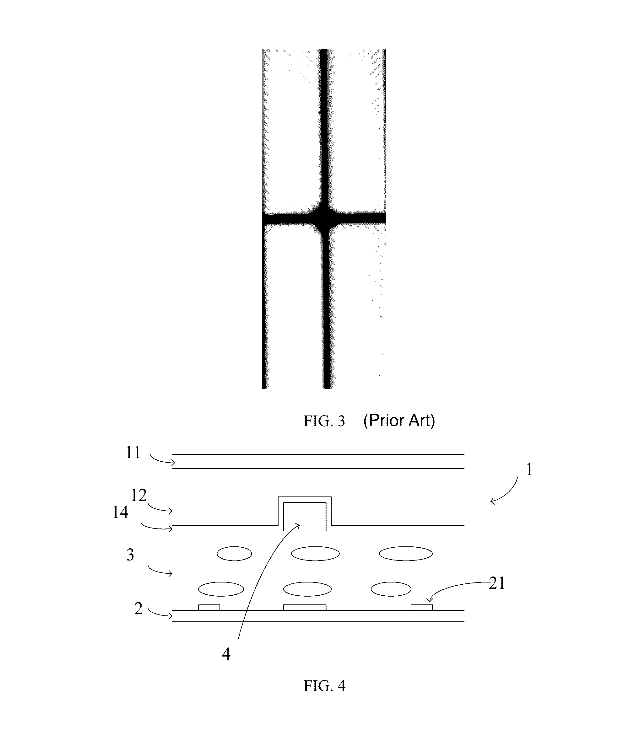
[0035]Referring to FIGS. 4 and 5, the liquid crystal panel includes a first substrate 2, a second substrate 1 arranged opposite to the first substrate 2, and a liquid crystal layer 3 between the second substrate 1 and the first substrate 2. As shown in FIG. 6, the first substrate 2 includes a plurality of pixels, and each of the pixel corresponds to one pixel electrode. The pixel electrode includes a plurality of primary electrodes 21 and a plurality of branch electrodes 22 extending from the primary electrodes 21. The primary electrode 21 divides the pixel into a plurality of areas. The branch electrodes 22 are arranged within the areas defined by the primary electrode 21. The primary electrode 21 may be two or more than two electrodes vertical to each other so as to define the pixel to four, six, or eight areas...


PUM

PropertyMeasurementUnit
widthaaaaaaaaaa
widthaaaaaaaaaa
shapeaaaaaaaaaa

Abstract

A liquid crystal panel is disclosed. The liquid crystal panel includes a first substrate, a second substrate, and a liquid crystal layer between the first substrate and the second substrate. The first substrate includes a plurality of pixels respectively corresponding to one pixel electrode. The pixel electrode includes a plurality of primary electrodes and a plurality of branch electrodes extending from the primary electrodes. The second substrate includes a base substrate and a common electrode layer formed on the base substrate. The common electrode layer includes a plurality of recessed portions facing toward the base substrate, and each of the recessed portions faces toward one corresponding primary electrode of the pixel electrode. In this way, the liquid crystal efficiency of pixels is enhanced and an applicable range of ultra-high-resolution, small-sized panels of VA mode may be extended.

Description

BACKGROUND OF THE INVENTION[0001]1. Field of the Invention[0002]The present disclosure relates to liquid crystal display technology, and more particularly to a liquid crystal panel.[0003]2. Discussion of the Related Art[0004]Vertical alignment (VA) thin-film transistor liquid crystal devices (TFT-LCDs) are characterized by attributes including high aperture rate, high resolution, and wide viewing angles, and thus are widely adopted by large-scale LCDs. As shown in FIG. 1, pixel electrodes of TFT array substrate of conventional VA mode LCDs are designed as fish-bones. That is, the electrode is divided into a plurality of display areas by primary electrodes vertical to each other. Each display area is configured with stripe-like branch electrodes spaced apart from each other. Referring to FIG. 2, the electrodes of color filter (CF) substrates are film-shaped operating as common electrode. The common electrodes of the pixel electrodes of FIGS. 1 and 2 are combined together to form the ...

Claims


Application Information

Patent Timeline
Patent Type & Authority Applications(United States)
IPC IPC(8): G02F1/1343G02F1/1335
CPCG02F1/134309G02F1/133514G02F2201/121G02F2201/123G02F2201/50G02F1/133707G02F1/134318
Inventor HAO, SIKUN
Owner SHENZHEN CHINA STAR OPTOELECTRONICS TECH CO LTD
Why Eureka
Try Eureka