Semiconductor device and method of manufacturing the same
a semiconductor and semiconductor technology, applied in the field of semiconductor devices, can solve the problems of increasing the resistance to the inside of the chip, increasing the chip area, increasing the cost of the chip, etc., and achieve the effects of reducing the power supply voltage drop, and reducing the increase in the chip area
- Summary
- Abstract
- Description
- Claims
- Application Information
AI Technical Summary
Benefits of technology
Problems solved by technology
Method used
Image

Examples
embodiment 1
[0049]A semiconductor device according to Embodiment 1 of the present invention includes external connection pads and test pads arranged in the central region of a chip. With this structure, the semiconductor device according to Embodiment 1 of the present invention reduces a power-supply voltage drop at the time of screening in a wafer state, while reducing an increase in the chip area.
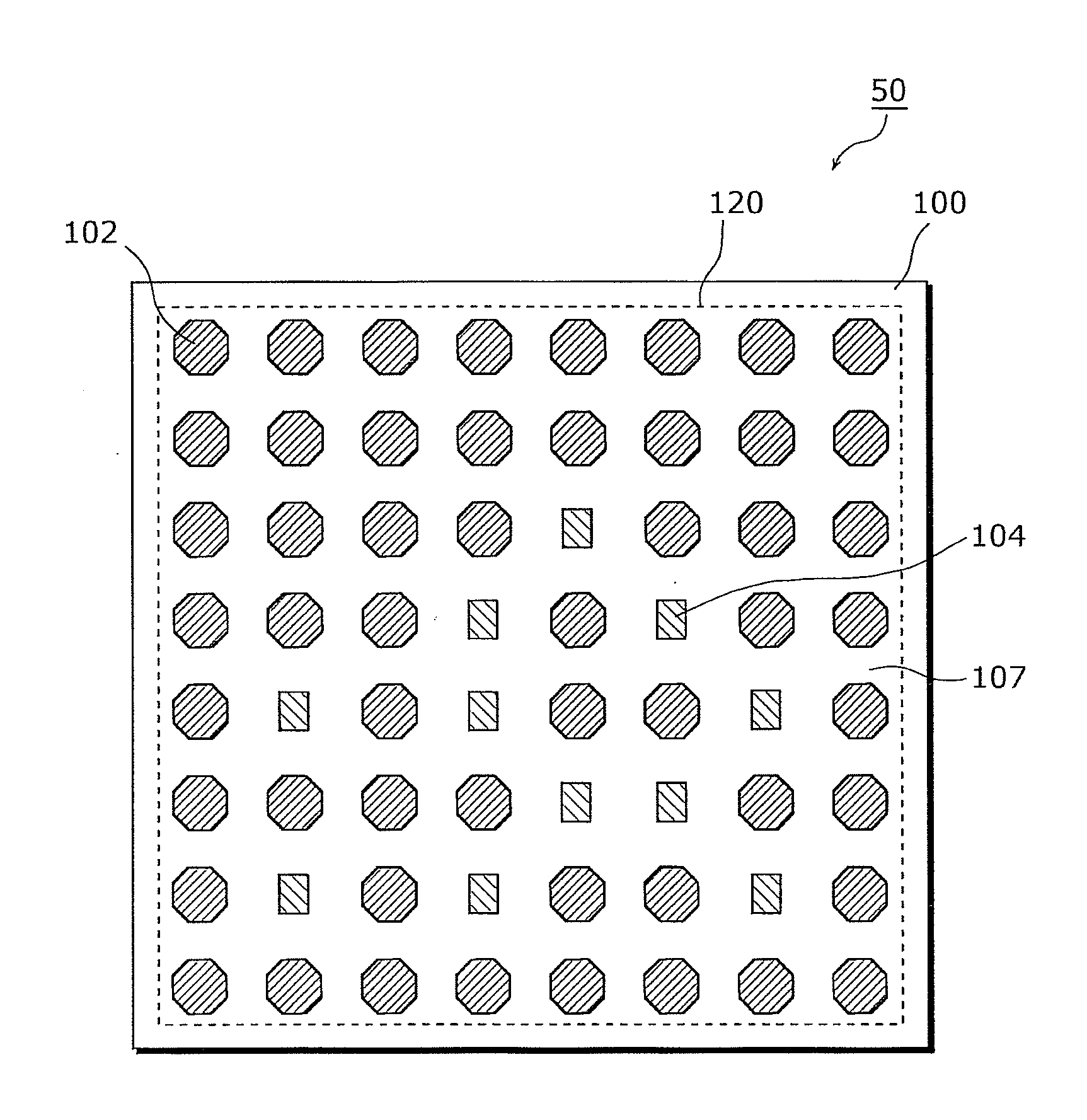
[0050]FIG. 1 is a diagram of a pad layout of a semiconductor device 50 according to Embodiment 1 of the present invention.
[0051]The semiconductor device 50 shown in FIG. 1 is a semiconductor integrated circuit used for packaging of surface mount such as an area array. The semiconductor device 50 includes a semiconductor chip 100, external connection pads 102, test pads 104, and a protective film 107.
[0052]The semiconductor chip 100 is formed of, for example, an Si substrate. The semiconductor chip 100 has an upper surface having a central region referred to as a chip central region 120.
[0053]In the c...
embodiment 2
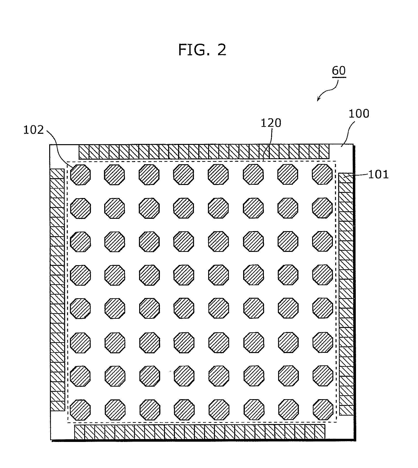
[0083]FIG. 8 is a diagram of a pad layout of a semiconductor device 53 according to Embodiment 2 of the present invention.
[0084]In the semiconductor device 53 shown in FIG. 8, similar to the semiconductor device 51 according to Embodiment 1, electrode pads are arranged in an area array in a chip central region 120 of a semiconductor chip 100. In the semiconductor device 51 according to Embodiment 1, electrode pads including the external connection pads 102 and the test pads 104 are arranged in an area array; however, in the semiconductor device 53 according to Embodiment 2, only external connection pads 102B are arranged in an area array, and test pads 104B are arranged in the spaces between adjacent external connection pads 102B arranged in the area array.
[0085]Similar to Embodiment 1, a probe test is performed by applying the probe needles 106 to the test pads 101 and 104B, and the bumps 105 are formed on the external connection pads 102B.
[0086]In the semiconductor device 53, the ...
embodiment 3
[0088]FIG. 9 is a diagram of a pad layout of a semiconductor device 54 according to Embodiment 3 of the present invention. The structure of the pad layout is the same as that in Embodiment 1.
[0089]The semiconductor device 54 shown in FIG. 9 further includes a plurality of circuit blocks 111 to 117 formed on the semiconductor chip 100.
[0090]The test pads 104 are arranged above the circuit block 114 having a greatest power consumption among the circuit blocks 111 to 117.
[0091]For example, the circuit block 114 is an ultra-high-speed processor which operates at a higher speed and consumes greater power compared to the other circuit blocks.
[0092]Similar to Embodiment 1, a probe test is performed by applying the probe needles 106 to the test pads 101 and 104, and then the bumps 105 are formed on the external connection pads 102.
[0093]In such a manner, at the time of the probe test, power-supply voltage is supplied also from the test pads 104; and thus, the circuit operation is stabilized...
PUM
 Abstract
Description
Claims
Application Information
 - R&D
- Intellectual Property
- Life Sciences
- Materials
- Tech Scout
- Unparalleled Data Quality
- Higher Quality Content
- 60% Fewer Hallucinations
Browse by: Latest US Patents, China's latest patents, Technical Efficacy Thesaurus, Application Domain, Technology Topic, Popular Technical Reports.
© 2025 PatSnap. All rights reserved.Legal|Privacy policy|Modern Slavery Act Transparency Statement|Sitemap|About US| Contact US: help@patsnap.com