
Probe card

a technology of a probe card and a spherical plate, which is applied in the direction of measurement devices, semiconductor/solid-state device testing/measurement, instruments, etc., can solve the problems of reducing throughput, requiring a long time, and unable to completely suppress the stress generated by thermal deformation

Inactive Publication Date: 2005-07-21
TOKYO ELECTRON LTD
View PDF10 Cites 17 Cited by
  • Summary
  • Abstract
  • Description
  • Claims
  • Application Information

AI Technical Summary

Benefits of technology

The present invention provides a probe card for testing the electrical characteristics of an object. The probe card has a contactor, a circuit board, an intermediate member, and a connecting member. The intermediate member is flexible and comes into contact with the contactor and circuit board, while the connecting member integrates the contactor, circuit board, and reinforcing member. The probe card may also have an elastic member, a reinforcing member, an elastically deformable contact, or a ceramic board. The technical effects of the invention include improved accuracy and reliability in testing electrical characteristics, as well as simplified and efficient assembly and maintenance of the probe card.

Problems solved by technology

However, the reinforcing member 5D cannot suppress stress generated by thermal deformation completely.
Preheating, however, requires a long time, and decreases throughput.

Method used


Image

  • Probe card
  • Probe card
  • Probe card

Examples


first embodiment

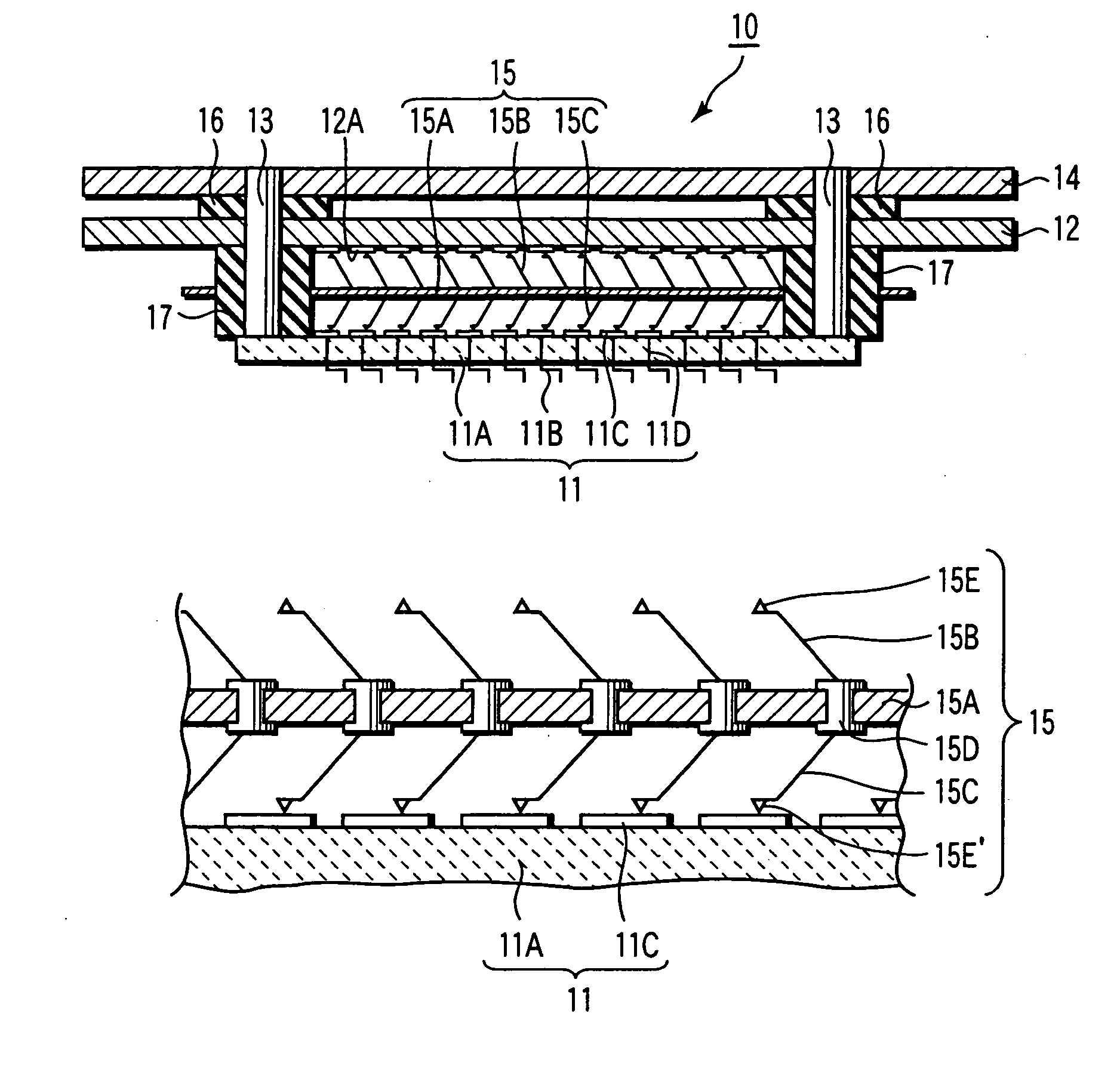
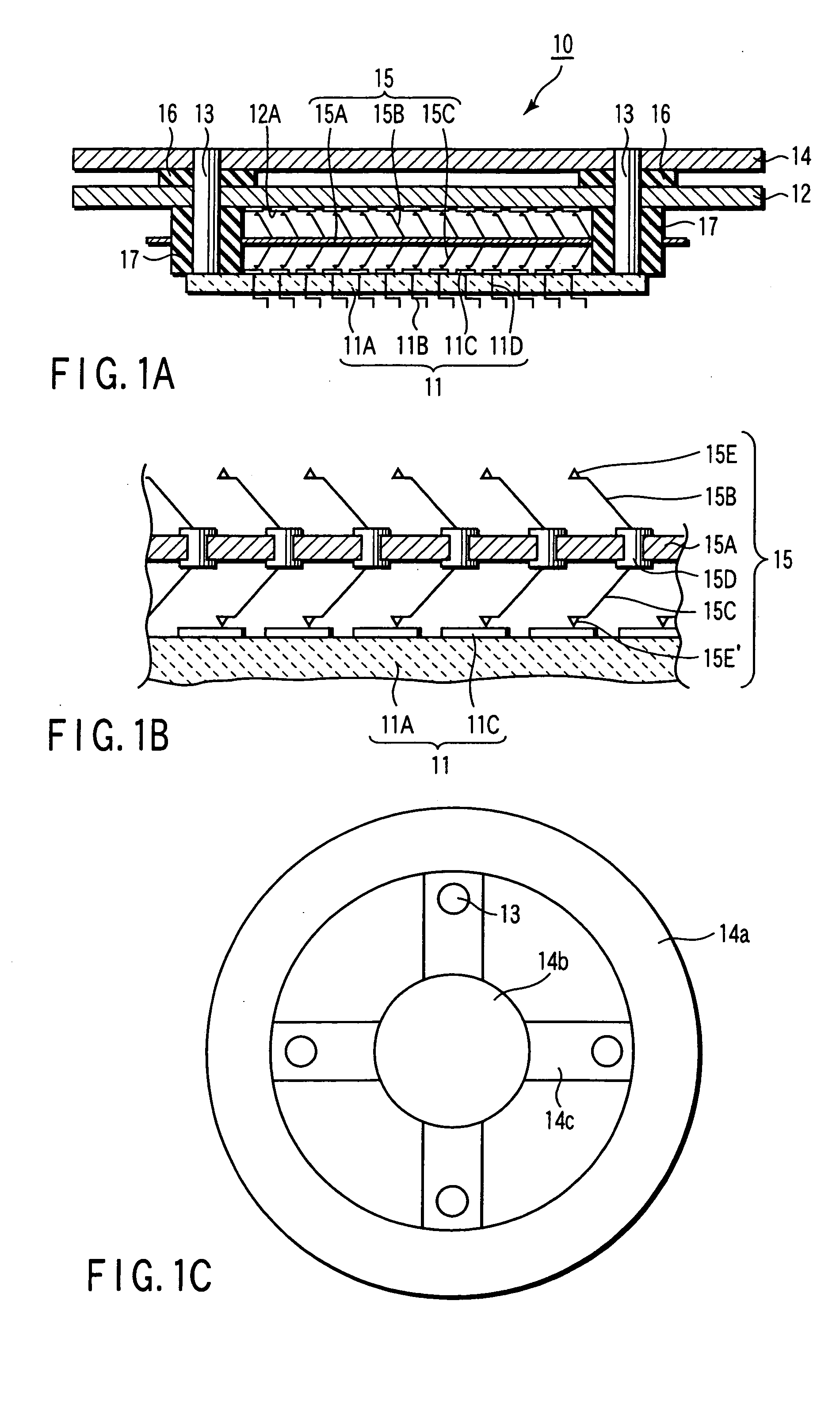
[0037] A probe card 10 according to the first embodiment shown in FIGS. 1A to 1C can have a contactor 11, intermediate member 15, circuit board 12, connecting member 13, and reinforcing member 14. The intermediate member 15 can also be referred to as an “interposer”. The circuit board (to be also referred to as a “printed wiring board” hereinafter) 12 is electrically connected to the contactor 11. The connecting member 13 connects the contactor 11 and printed wiring board 12 to integrate them. The reinforcing member 14 reinforces the printed wiring board 12 integrated by the connecting member 13.

[0038] As shown in FIGS. 1A and 1B, the contactor 11 can have a ceramic board 11A, a plurality of probes 11B, terminal electrodes 11C, and connecting wirings 11D. The ceramic board 11A is made of, e.g., a ceramic material. The probes 11B are formed on the lower surface of the ceramic board 11A. The terminal electrodes 11C are formed on the upper surface of the ceramic board 11A. The connect...

second embodiment

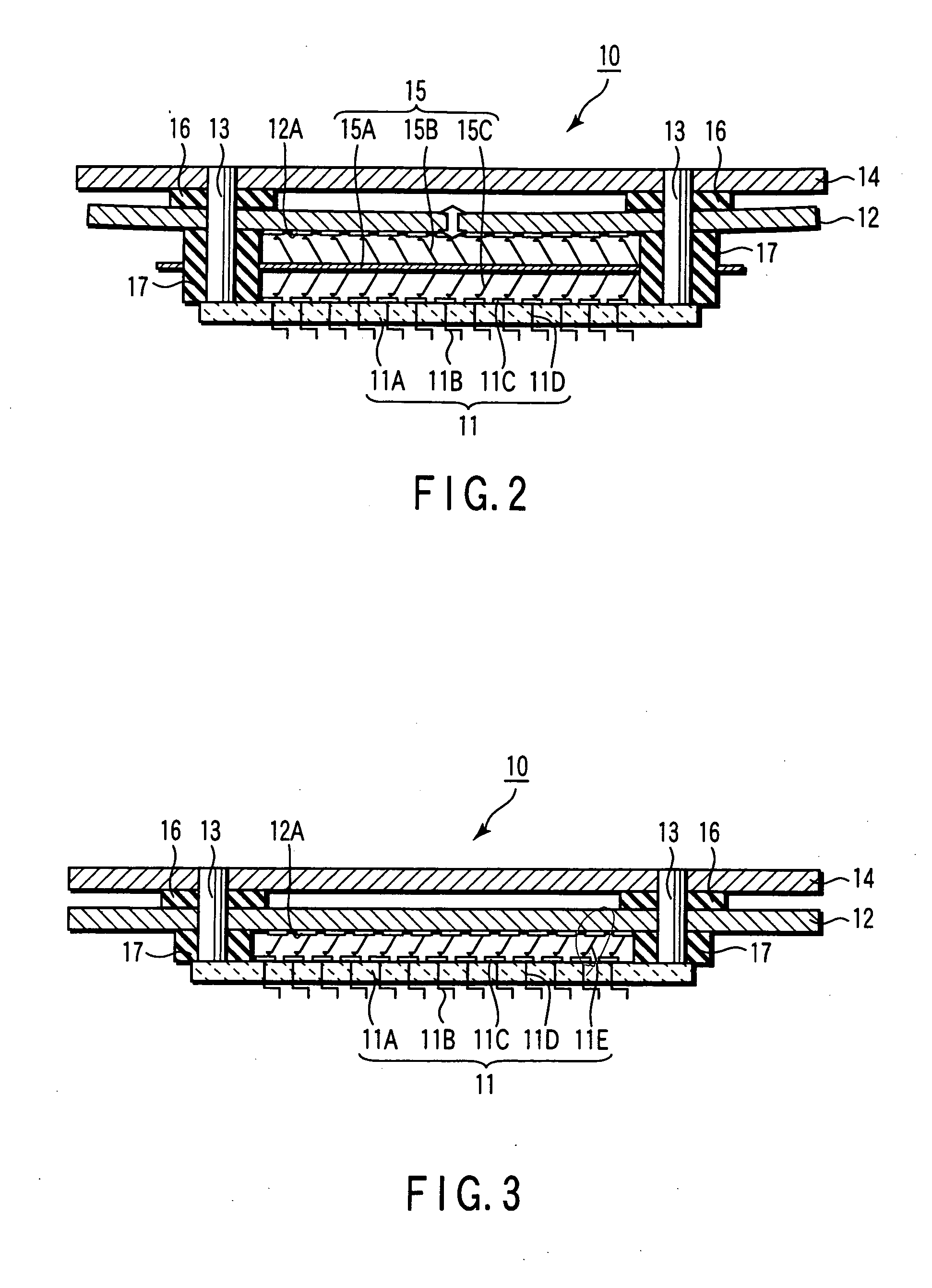
[0050] A probe card 10 of the second embodiment can have, as an intermediate member, a plurality of elastically deformable contacts 11E arranged on the upper surface of a contactor 11, as shown in, e.g., FIG. 3, in place of the intermediate member 15 shown in FIGS. 1 and 2.

[0051] The contacts 11E can be formed in the same manner as the contacts 15C of the interposer 15 shown in FIG. 1B. As shown in FIG. 3, the contacts 11E can be directly fixed to terminal electrodes 11C formed on the. upper surface of a ceramic board 11A of the contactor 11. The contactor 11 comes into electrical contact with terminal electrodes 12A of a printed wiring board 12 through the plurality of contacts 11E.

[0052] According to this embodiment, even when the printed wiring board 12 is deformed by thermal expansion, the thermal deformation can be absorbed by the contacts 11E of the contactor 11. This embodiment can provide the same operation and effect as those of the first embodiment. According to this emb...


PUM


Abstract

A probe card of this invention includes a contactor, printed wiring board, interposer, connecting member, and reinforcing member. The interposer is arranged between the contactor and printed wiring board to bring the contactor and printed wiring board into contact with each other flexibly and electrically. The connecting member integrates the contactor, printed wiring board, and interposer. The reinforcing member reinforces the printed wiring board integrated through the connecting member.

Description

CROSS-REFERENCE TO RELATED APPLICATIONS [0001] This application is based upon and claims the benefit of priority from prior Japanese Patent Application No. 2004-012077, filed Jan. 20, 2004, the entire contents of which are incorporated herein by reference. BACKGROUND OF THE INVENTION [0002] 1. Field of the Invention [0003] The present invention relates to a probe card used to test the electrical characteristics of an object to be tested such as a semiconductor element (to be described as a “device” hereinafter) formed on a wafer. More particularly, the present invention relates to a probe card capable of performing highly reliable testing even after it has become thermally deformed. [0004] 2. Description of the Related Art [0005] A probe card is used in, e.g., a prober shown in FIG. 4. As shown in FIG. 4, the prober has a loader chamber 1 and a prober chamber 2. A wafer W is transported from the loader chamber 1. In the prober chamber 2, the electrical characteristics of a device or...

Claims


Application Information

Patent Timeline
Patent Type & Authority Applications(United States)
IPC IPC(8): H01L21/66G01R1/073
CPCG01R1/07342H01L22/00
Inventor HOSAKA, HISATOMI
Owner TOKYO ELECTRON LTD
Learn More