
Metal foil interconnection of electrical devices

a technology of metal foil and electrical devices, which is applied in the direction of solid-state devices, semiconductor/solid-state device details, manufacturing tools, etc., can solve the problems of poor ic reliability, ic failure and even explosive failure of the ic, interconnection failure, and increase the cost, volume and weight of the ic, so as to reduce the resistance increase the reliability of the interconnecting element.

Active Publication Date: 2011-11-17
RAYTHEON CO
View PDF4 Cites 2 Cited by
  • Summary
  • Abstract
  • Description
  • Claims
  • Application Information

AI Technical Summary

Benefits of technology

This solution reduces parasitic inductance and resistance, enhancing the reliability and performance of electrical interconnections by minimizing thermal heating and stress at bond locations, and allowing for more efficient current distribution.

Problems solved by technology

Undesirable parasitics, such as, parasitic inductance and parasitic resistance, associated with wire bond interconnection, can induce large voltage and current spikes in the IC leading to poor IC reliability, IC failure and even explosive failure of the IC.
To compensate for interconnection parasitics, it has been necessary to over-design power IC circuits with increased design margins and this has lead to reduce power efficiencies and increases in the cost, volume and weight of the ICs.
Another problem caused by the rapid on-off current flow over conventional interconnecting wire bonds is that the bond wires are susceptible to rapidly varying electro-thermal-mechanical stress which can lead to interconnection failures.
In particular, rapid changes in current flow produce rapid heating and therefore rapid thermal expansion and contraction of the larger diameter relatively stiff wire material.
This action can lead to fatigue failure at the wire bond contact points which will lead to increased current and therefore stress on remaining bond connections, thereby reducing the reliability of the overall electrical system.

Method used


Image

  • Metal foil interconnection of electrical devices
  • Metal foil interconnection of electrical devices
  • Metal foil interconnection of electrical devices

Examples


Embodiment Construction

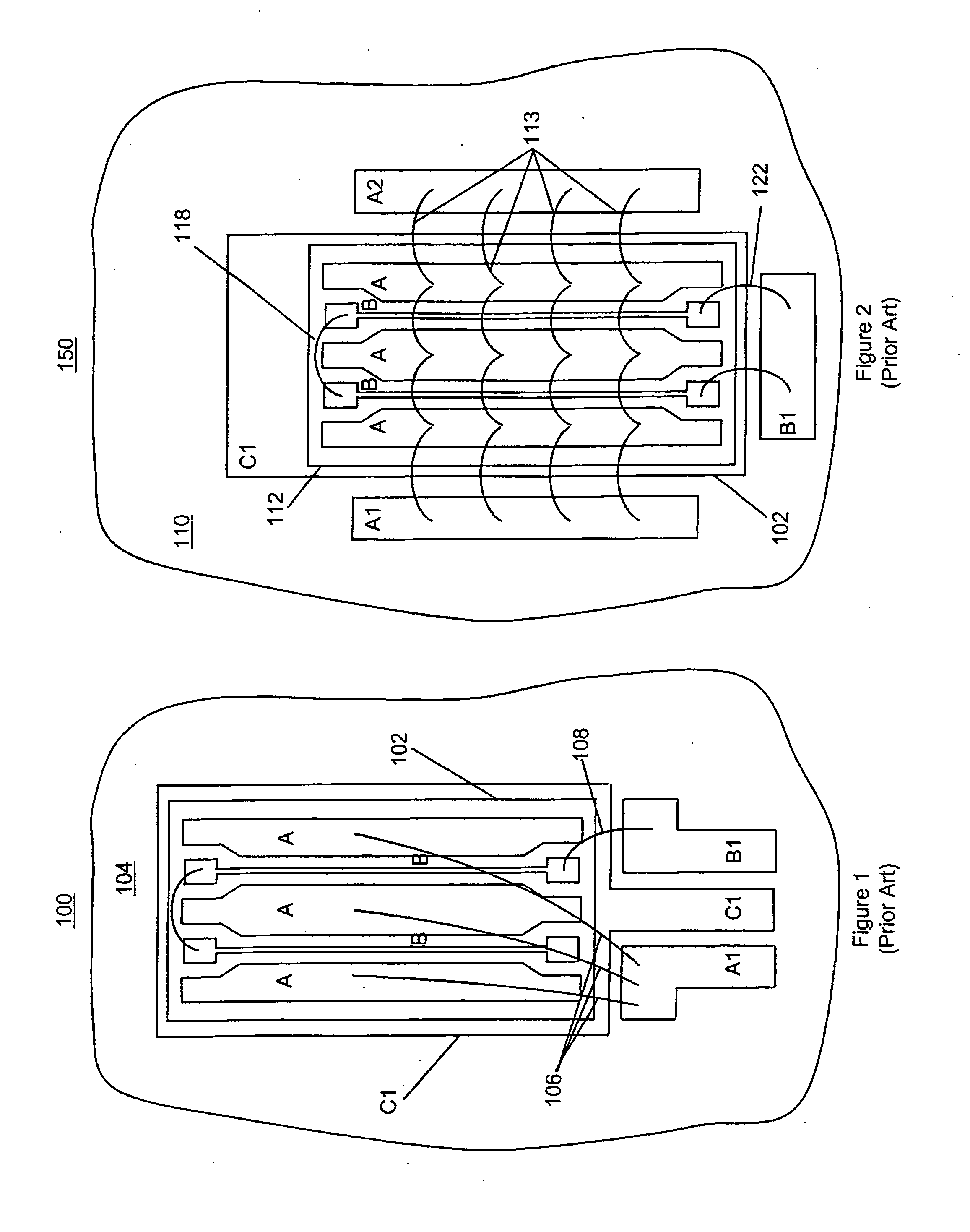
[0038]Referring to FIG. 1 a schematic representation of a first embodiment 100 of a conventional unpackaged electronic device 102 e.g. an integrated circuit (IC) or chip, supported on a substrate module 104 is shown in top view. An outer package or housing, not shown, supports and protects the electronic device 102 and substrate module 104 against moisture and contaminates as well as provides an electromagnetic shield.

[0039]The electronic device 102 includes a plurality of conductive device surfaces A and B, disposed on a top surface of the device 102 and a conductive device surface C, not shown, on the bottom surface of the device 102. Alternately, or additionally, other conductive device surfaces may be disposed on other surfaces of the packaged electronic device 102. Each conductive device surface A, B, and C comprises a conductive metal, e.g. aluminum, or a conductive bondable material, or the like suitable for collecting surface charges thereon and or conducting current thereth...


PUM


Abstract

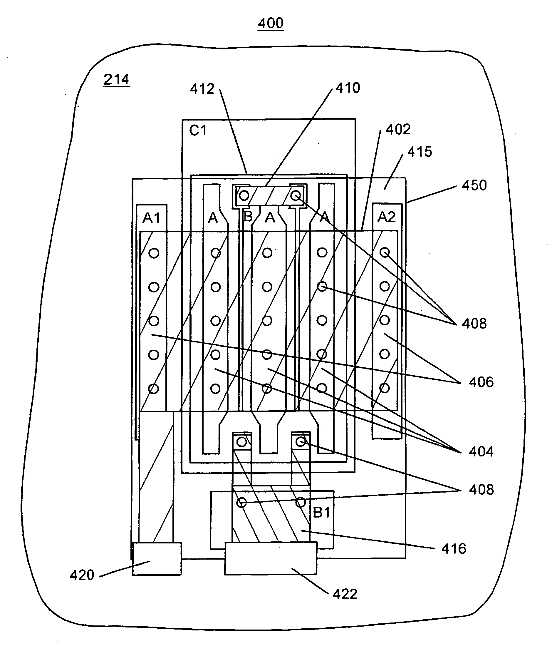
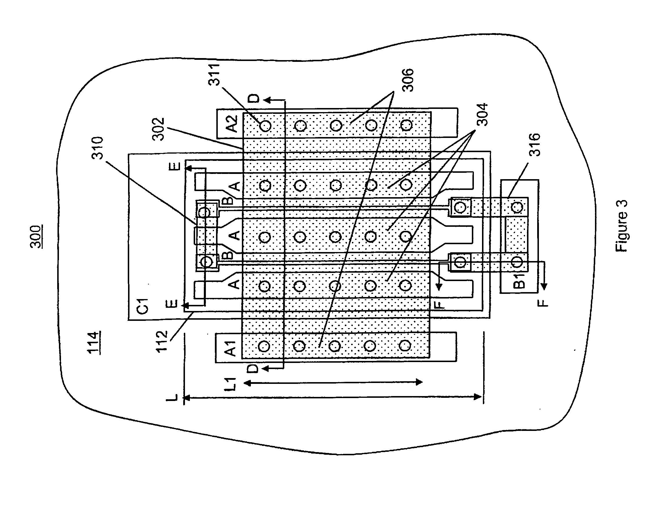
An electrical assembly (300, 400) includes a power IC such as a MOSFET (112, 412) attached to a substrate module (114, 214). The MOSFET includes a top surface comprising first and second conductive device surfaces (A, B), associated with first and second device ports, and a bottom surface comprising a third conductive device surface C associated with a third device port. A first foil element is bonded to the first conductive device surface(s) A and to each of the first conductive substrate surfaces (A1, A2) and provides a continuous conductive pathway from each conductive surface (A) to each other conductive surface (A) and to each conductive surface (A1, A2). A second foil element is bonded to the second conductive device surface(s) B and to the second conductive substrate surface B1 and provides a continuous conductive pathway from each device conductive surface (B) to the substrate conductive surface (B1). A third foil element may be installed to electrically interconnect the discrete second device surfaces (B). The foil elements reduce interconnection parasitics and reduce charge and thermal energy density at device conductive surfaces as compared to wire bonded electrical interconnections. The foil elements may be comprised of formed metal elements that are flexible but sufficiently rigid to hold a formed shape or flexible foils supported on a flexible dielectric substrate.

Description

RELATED APPLICATIONS[0001]This application is a divisional application of U.S. patent application Ser. No. 11 / 998,670 filed Nov. 30, 2007, under 35 U.S.C. §§119, 120, 363, 365, and 37 C.F.R. §1.55 and §1.78, which is incorporated by reference herein.FIELD OF THE INVENTION[0002]The present invention relates to an improved method and apparatus for making electrical interconnects between power semiconductor devices and a substrate module and specifically to interconnecting power semiconductor devices with a substrate module using a formed conductive foil element or a formed flexible interconnection assembly comprised of a supporting dielectric film and conductive foil elements.DESCRIPTION OF THE RELATED ART[0003]Power semiconductor devices, or power integrated circuits (ICs), used as switches or rectifiers in power electronic circuits, and the like, often operate at considerably higher Power and current density levels than other semiconductor devices.[0004]Generally power ICs are enclo...

Claims


Application Information

Patent Timeline
Patent Type & Authority Applications(United States)
IPC IPC(8): B23K31/02
CPCH01L23/49844H01L24/36H01L24/40H01L24/45H01L24/49H01L24/84H01L2224/45014H01L2224/45015H01L2224/45124H01L2224/48091H01L2224/4813H01L2224/48132H01L2224/48227H01L2224/4911H01L2224/49113H01L2224/49171H01L2224/49175H01L2224/83205H01L2224/85424H01L2224/85455H01L2924/01005H01L2924/01013H01L2924/01027H01L2924/01028H01L2924/01029H01L2924/01074H01L2924/01078H01L2924/01079H01L2924/01082H01L2924/13055H01L2924/13091H01L2924/14H01L2924/2076H01L2924/30107H01L2924/3025H01L24/48H01L2924/01006H01L2924/01033H01L2924/014H01L2224/37124H01L2224/37147H01L2924/1306H01L2924/1301H01L2924/1305Y10T29/49165Y10T29/4913Y10T29/49144Y10T29/49158H01L2924/00014H01L2924/00H01L2924/351H01L2224/45147H01L2224/48824H01L2224/48855H01L2224/48724H01L2224/48755H01L2224/40095H01L2224/84205H01L2224/40225H01L24/37H01L2224/83801H01L2924/20755H01L2924/00015H01L2924/2075H01L2924/20754H01L2924/206H01L2224/73221
Inventor GUINN, KEITH V.
Owner RAYTHEON CO
Learn More