Integrated circuit device

a circuit device and integrated circuit technology, applied in the direction of electric variable regulation, process and machine control, instruments, etc., can solve the problem of difficulty in down-sizing the entire device, and achieve the effect of efficient driving and efficient boos

Inactive Publication Date: 2011-10-27
THE UNIV OF TOKYO
View PDF3 Cites 28 Cited by
  • Summary
  • Abstract
  • Description
  • Claims
  • Application Information

AI Technical Summary

Benefits of technology

[0013]In the integrated circuit device that the voltage boosting supply circuit has the boost converter and the switching control circuit controlling the switching of the switching element using the pulse signal according to this aspect of the invention, the switching control circuit includes a voltage detection unit for detecting a voltage of the input terminal and the switching control unit controls the switching of the switching element by using a pulse signal with a frequency and a duty ratio adjusted with respect to the detected voltage so that the boost converter can driven efficiently. This arrangement desirably boosts efficiently regardless of the fluctuation of the voltage of the input terminal.

Problems solved by technology

So it is difficult to perform down-sizing the entire device.

Method used


Image

  • Integrated circuit device
  • Integrated circuit device
  • Integrated circuit device

Examples


Embodiment Construction

[0035]One mode of carrying out the invention is described below as a preferred embodiment.

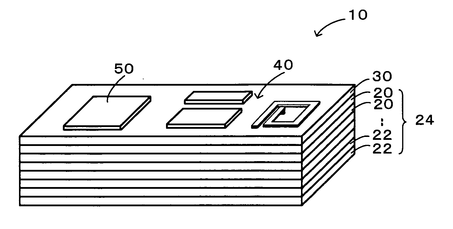
[0036]FIG. 1 schematically illustrates the configuration of an integrated circuit device 10 that a SSD (Solid State Disk) is equipped with as an internal storage of a computer of one embodiment of the invention. The integrated circuit device 10 has a stacked structure 24 formed by stacking a plurality of a DRAM (Dynamic Random Access Memory) chip 20 that is a silicon chip formed DRAM and a plurality of a flash memory chip 22 that is a silicon chip formed NAND-type flash memory, and an interposer 30 disposed on an upper surface of the stacked structure 24. The integrated circuit device 10 is supplied a voltage V1 (for example, 1.8V) as a power-supply voltage from an external power supply not illustrated. In this embodiment, DRAM chip 20 is operated at the voltage V1. A program-voltage for writing of the NAND-type flash memory is the voltage V1 and a readout voltage of the NAND type flash memory ...


PUM


Abstract

The interposer is disposed on an upper surface of the stacked structure formed by stacking a plurality of a DRAM chip and a plurality of a flash memory chip. Thus down-size of an entire device is accomplished. A boost converter having an inductor is used as a voltage boost circuit. Thus down-size of the entire device is accomplished in comparison to a voltage boost circuit using a charge pump connected in parallel with a plurality of a capacitance.

Description

TECHNICAL FIELD[0001]The present invention relates to an integrated circuit device, for details, an integrated circuit device including a stacked structure formed by stacking a plurality of integrated circuit chips including a first integrated circuit chip having a first integrated circuit operated at a first voltage.BACKGROUND ART[0002]A proposed structure of an integrated circuit device includes a stacked structure formed by stacking f a plurality of flash memory chips having flush memory (see, for example, Non-Patent Document 1). This proposed integrated circuit device successively performs down-sizing the device by stacking a plurality of flash memory chips.[0003]Non-Patent Document 1: Tanaka et al. “NAND-type flash Memory”, TOSHIBA REVIEW, 2008. vol. 63 No 2. pp. 28-31.DISCLOSURE OF THE INVENTION[0004]In this prior art integrated circuit device, a voltage boosting supply circuit for boosting a power-supply voltage to a program-voltage for writing data is needed because the prog...

Claims


Application Information

Patent Timeline
IPC IPC(8): G05F1/10
CPCG11C5/02G11C5/04H01L2924/0002G11C5/145G11C11/005G11C16/12G11C16/30H01L25/0657H01L25/16H01L25/18H01L2225/06513H01L2225/06517H01L2924/19106H01L2924/00
Inventor TAKEUCHI, KENYASUFUKU, TADASHIISHIDA, KOICHITAKAMIYA, MAKOTOSAKURAI, TAKAYASU
Owner THE UNIV OF TOKYO
Why Eureka
Try Eureka